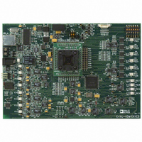
EVAL-ADM1063TQEBZ Analog Devices Inc, EVAL-ADM1063TQEBZ Datasheet - Page 16
EVAL-ADM1063TQEBZ
Manufacturer Part Number
EVAL-ADM1063TQEBZ
Description
BOARD EVALUATION FOR ADM1063TQ
Manufacturer
Analog Devices Inc
Specifications of EVAL-ADM1063TQEBZ
Main Purpose
Power Management, Power Supply Supervisor/Tracker/Sequencer
Embedded
No
Utilized Ic / Part
ADM1063
Primary Attributes
10 Channel Supervisor / Sequencer, 6 Voltage Output DACs
Secondary Attributes
GUI Programmable via SMBus (via USB)
Lead Free Status / RoHS Status
Lead free / RoHS Compliant


ADM1063
OUTPUTS
SUPPLY SEQUENCING THROUGH
CONFIGURABLE OUTPUT DRIVERS
Supply sequencing is achieved with the ADM1063 using the
programmable driver outputs (PDOs) on the device as control
signals for supplies. The output drivers can be used as logic
enables or as FET drivers.
The sequence in which the PDOs are asserted (and, therefore,
the supplies are turned on) is controlled by the sequencing engine
(SE). The SE determines what action is taken with the PDOs,
based on the condition of the ADM1063 inputs. Therefore, the
PDOs can be set up to assert when the SFDs are in tolerance, the
correct input signals are received on the VXx digital pins, no
warnings are received from any of the inputs of the device, and
at other times. The PDOs can be used for a variety of functions.
The primary function is to provide enable signals for LDOs or
dc-to-dc converters that generate supplies locally on a board.
The PDOs can also be used to provide a PWRGD signal, when all
the SFDs are in tolerance, or a RESET output if one of the SFDs
goes out of specification (this can be used as a status signal for a
DSP, FPGA, or other microcontroller).
The PDOs can be programmed to pull up to a number of different
options. The outputs can be programmed as follows:
•
•
•
•
•
•
•
The last option (available only on PDO1 to PDO6) allows the
user to directly drive a voltage high enough to fully enhance an
external N-FET, which is used to isolate, for example, a card-
side voltage from a backplane supply (a PDO can sustain greater
than 10.5 V into a 1 μA load). The pull-down switches can also
be used to drive status LEDs directly.
The data driving each of the PDOs can come from one of three
sources. The source can be enabled in the PDOxCFG configuration
Open drain (allowing the user to connect an external
pull-up resistor).
Open drain with weak pull-up to V
Open drain with strong pull-up to V
Open drain with weak pull-up to VPx.
Open drain with strong pull-up to VPx.
Strong pull-down to GND.
Internally charge-pumped high drive (12 V, PDO1 to
PDO6 only).
SMBus DATA
CLK DATA
SE DATA
CFG4 CFG5 CFG6
DD
DD
.
.
Figure 22. Programmable Driver Output
Rev. B | Page 16 of 32
SEL
VP1
register (see the AN-698 Application Note at
details).
The data sources are as follows:
•
•
•
DEFAULT OUTPUT CONFIGURATION
All of the internal registers in an unprogrammed ADM1063 device
from the factory are set to 0. Because of this, the PDOx pins are
pulled to GND by a weak (20 kΩ) on-chip pull-down resistor.
As the input supply to the ADM1063 ramps up on VPx or VH,
all PDOx pins behave as follows:
•
•
•
The internal pull-down can be overdriven with an external pull-
up of suitable value tied from the PDOx pin to the required pull-up
voltage. The 20 kΩ resistor must be accounted for in calculating
a suitable value. For example, if PDOx must be pulled up to 3.3 V,
and 5 V is available as an external supply, the pull-up resistor
value is given by
Therefore,
Output from the SE.
Directly from the SMBus. A PDO can be configured so that
the SMBus has direct control over it. This enables software
control of the PDOs. Therefore, a microcontroller can be
used to initiate a software power-up/power-down sequence.
On-chip clock. A 100 kHz clock is generated on the device.
This clock can be made available on any of the PDOs. It
can be used, for example, to clock an external device such
as an LED.
Input supply = 0 V to 1.2 V. The PDOs are high impedance.
Input supply = 1.2 V to 2.7 V. The PDOs are pulled to GND
by a weak (20 kΩ) on-chip pull-down resistor.
Supply > 2.7 V. Factory programmed devices continue to
pull all PDOs to GND by a weak (20 kΩ) on-chip pull-down
resistor. Programmed devices download current EEPROM
configuration data, and the programmed setup is latched. The
PDO then goes to the state demanded by the configuration.
This provides a known condition for the PDOs during
power-up.
3.3 V = 5 V × 20 kΩ/(R
R
UP
VP4
= (100 kΩ − 66 kΩ)/3.3 V = 10 kΩ
V
DD
VFET (PDO1 TO PDO6 ONLY)
UP
+ 20 kΩ)
PDO
www.analog.com
for
Related parts for EVAL-ADM1063TQEBZ
Image
Part Number
Description
Manufacturer
Datasheet
Request
R

Part Number:
Description:
IC, ADJ LDO REG, 1.5V TO 5V 250mA MSOP-8
Manufacturer:
Vishay
Datasheet:

Part Number:
Description:
IC, ADJ LDO REG, 1.5V TO 5V 0.6A 8-TSSOP
Manufacturer:
Vishay
Datasheet:
Part Number:
Description:
IC, ADJ LDO REG, 1.5V TO 5V 250mA MSOP-8
Manufacturer:
Vishay
Datasheet:

Part Number:
Description:
IC ADJ LDO REG 1.5V TO 5V 150mA 5-SOT-23
Manufacturer:
Vishay
Datasheet:

Part Number:
Description:
BOARD EVAL AS1324-AD
Manufacturer:
austriamicrosystems
Datasheet:
Part Number:
Description:
IC, ADJ LDO REG, 1.5V TO 5V 0.6A 8-TSSOP
Manufacturer:
Vishay
Datasheet:

Part Number:
Description:
IC, ADJ LDO REG, 1.5V TO 5V, 0.3A, MSOP8
Manufacturer:
Vishay
Datasheet:
Part Number:
Description:
IC, ADJ LDO REG, 1.5V TO 5V, 0.3A, MSOP8
Manufacturer:
Vishay
Datasheet:
Part Number:
Description:
IC, ADJ LDO REG 1.215V TO 5V 0.3A MSOP-8
Manufacturer:
Vishay
Datasheet:
Part Number:
Description:
IC, ADJ LDO REG 1.215V TO 5V 0.3A MSOP-8
Manufacturer:
Vishay
Datasheet:

Part Number:
Description:
±1.7g Dual-Axis IMEMS Accelerometer Evaluation Board
Manufacturer:
Analog Devices Inc
Datasheet:

Part Number:
Description:
IC MULTIPLIER ANALOG 8-SOIC T/R
Manufacturer:
Analog Devices Inc
Datasheet:

Part Number:
Description:
IC ANALOG MULTIPLIER 8-DIP
Manufacturer:
Analog Devices Inc
Datasheet:
Part Number:
Description:
IC ANALOG MULTIPLIER 8-SOIC
Manufacturer:
Analog Devices Inc
Datasheet:
Part Number:
Description:
IC ANALOG MULTIPLIER 8-DIP
Manufacturer:
Analog Devices Inc
Datasheet: