EVAL-ADM1064TQEB Analog Devices Inc, EVAL-ADM1064TQEB Datasheet - Page 26
EVAL-ADM1064TQEB
Manufacturer Part Number
EVAL-ADM1064TQEB
Description
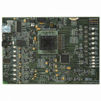
BOARD EVALUATION FOR ADM1064TQ
Manufacturer
Analog Devices Inc
Specifications of EVAL-ADM1064TQEB
Main Purpose
Power Management, Power Supply Supervisor/Tracker/Sequencer
Embedded
No
Utilized Ic / Part
ADM1064
Primary Attributes
10 Channel Supervisor / Sequencer, 6 Voltage Output DACs
Secondary Attributes
GUI Programmable via SMBus (via USB)
Lead Free Status / RoHS Status
Contains lead / RoHS non-compliant


ADM1064
SMBus PROTOCOLS FOR RAM AND EEPROM
The ADM1064 contains volatile registers (RAM) and nonvolatile
registers (EEPROM). User RAM occupies Address 0x00 to
Address 0xDF; the EEPROM occupies Address 0xF800 to
Address 0xFBFF.
Data can be written to and read from both the RAM and the
EEPROM as single data bytes. Data can be written only to
unprogrammed EEPROM locations. To write new data to a
programmed location, the location contents must first be erased.
EEPROM erasure cannot be done at the byte level. The EEPROM
is arranged as 32 pages of 32 bytes each, and an entire page must
be erased.
Page erasure is enabled by setting Bit 2 in the UPDCFG register
(Address 0x90) to 1. If this bit is not set, page erasure cannot occur,
even if the command byte (0xFE) is programmed across the
SMBus.
WRITE OPERATIONS
The SMBus specification defines several protocols for different
types of read and write operations. The following abbreviations
are used in Figure 34 to Figure 42:
•
•
•
•
•
•
The ADM1064 uses the following SMBus write protocols.
Send Byte
In a send byte operation, the master device sends a single
command byte to a slave device, as follows:
1.
2.
3.
4.
5.
6.
In the ADM1064, the send byte protocol is used for two
purposes:
•
S = Start
P = Stop
R = Read
W = Write
A = Acknowledge
A = No acknowledge
The master device asserts a start condition on SDA.
The master sends the 7-bit slave address followed by the
write bit (low).
The addressed slave device asserts an acknowledge (ACK)
on SDA.
The master sends a command code.
The slave asserts an ACK on SDA.
The master asserts a stop condition on SDA, and the
transaction ends.
To write a register address to the RAM for a subsequent
single byte read from the same address, or for a block read
or a block write starting at that address, as shown in Figure 34.
Figure 34. Setting a RAM Address for Subsequent Read
S
1
ADDRESS
SLAVE
2
W
A
3
(0x00 TO 0xDF)
ADDRESS
RAM
4
5
A
P
6
Rev. C | Page 26 of 32
•
Write Byte/Word
In a write byte/word operation, the master device sends a
command byte and one or two data bytes to the slave device,
as follows:
1.
2.
3.
4.
5.
6.
7.
8.
9.
10. The master asserts a stop condition on SDA to end the
In the ADM1064, the write byte/word protocol is used for three
purposes:
•
To erase a page of EEPROM memory. EEPROM memory
can be written to only if it is unprogrammed. Before writing
to one or more EEPROM memory locations that are already
programmed, the page(s) containing those locations must
first be erased. EEPROM memory is erased by writing a
command byte.
As soon as the ADM1064 receives the command byte,
page erasure begins. The master device can send a stop
command as soon as it sends the command byte. Page
erasure takes approximately 20 ms. If the ADM1064 is
accessed before erasure is complete, it responds with a
no acknowledge (NACK).
The master device asserts a start condition on SDA.
The master sends the 7-bit slave address followed by the
write bit (low).
The addressed slave device asserts an ACK on SDA.
The master sends a command code.
The slave asserts an ACK on SDA.
The master sends a data byte.
The slave asserts an ACK on SDA.
The master sends a data byte or asserts a stop condition.
The slave asserts an ACK on SDA.
transaction.
To write a single byte of data to the RAM. In this case, the
command byte is RAM Address 0x00 to RAM Address 0xDF,
and the only data byte is the actual data, as shown in Figure 36.
The master sends a command code telling the slave device to
erase the page. The ADM1064 command code for a page
erasure is 0xFE (1111 1110). Note that for a page erasure to
take place, the page address must be given in the previous
write word transaction (see the Write Byte/Word section).
In addition, Bit 2 in the UPDCFG register (Address 0x90)
must be set to 1.
S
1
S
1
ADDRESS
SLAVE
ADDRESS
SLAVE
Figure 36. Single Byte Write to the RAM
2
2
Figure 35. EEPROM Page Erasure
W A
3
W
(0x00 TO 0xDF)
A
ADDRESS
3
RAM
4
COMMAND
(0xFE)
BYTE
4
5
A
DATA
6
A
5
A
7
6
P
8
P
Related parts for EVAL-ADM1064TQEB
Image
Part Number
Description
Manufacturer
Datasheet
Request
R

Part Number:
Description:
IC, ADJ LDO REG, 1.5V TO 5V 250mA MSOP-8
Manufacturer:
Vishay
Datasheet:

Part Number:
Description:
IC, ADJ LDO REG, 1.5V TO 5V 0.6A 8-TSSOP
Manufacturer:
Vishay
Datasheet:
Part Number:
Description:
IC, ADJ LDO REG, 1.5V TO 5V 250mA MSOP-8
Manufacturer:
Vishay
Datasheet:

Part Number:
Description:
IC ADJ LDO REG 1.5V TO 5V 150mA 5-SOT-23
Manufacturer:
Vishay
Datasheet:

Part Number:
Description:
BOARD EVAL AS1324-AD
Manufacturer:
austriamicrosystems
Datasheet:
Part Number:
Description:
IC, ADJ LDO REG, 1.5V TO 5V 0.6A 8-TSSOP
Manufacturer:
Vishay
Datasheet:

Part Number:
Description:
IC, ADJ LDO REG, 1.5V TO 5V, 0.3A, MSOP8
Manufacturer:
Vishay
Datasheet:
Part Number:
Description:
IC, ADJ LDO REG, 1.5V TO 5V, 0.3A, MSOP8
Manufacturer:
Vishay
Datasheet:
Part Number:
Description:
IC, ADJ LDO REG 1.215V TO 5V 0.3A MSOP-8
Manufacturer:
Vishay
Datasheet:
Part Number:
Description:
IC, ADJ LDO REG 1.215V TO 5V 0.3A MSOP-8
Manufacturer:
Vishay
Datasheet:

Part Number:
Description:
±1.7g Dual-Axis IMEMS Accelerometer Evaluation Board
Manufacturer:
Analog Devices Inc
Datasheet:

Part Number:
Description:
IC MULTIPLIER ANALOG 8-SOIC T/R
Manufacturer:
Analog Devices Inc
Datasheet:

Part Number:
Description:
IC ANALOG MULTIPLIER 8-DIP
Manufacturer:
Analog Devices Inc
Datasheet:
Part Number:
Description:
IC ANALOG MULTIPLIER 8-SOIC
Manufacturer:
Analog Devices Inc
Datasheet:
Part Number:
Description:
IC ANALOG MULTIPLIER 8-DIP
Manufacturer:
Analog Devices Inc
Datasheet: