CDB48500-USB Cirrus Logic Inc, CDB48500-USB Datasheet - Page 35
CDB48500-USB
Manufacturer Part Number
CDB48500-USB
Description
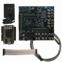
KIT USB EVALUATION FOR CDB48500
Manufacturer
Cirrus Logic Inc
Datasheet
1.CDB48500-USB.pdf
(52 pages)
Specifications of CDB48500-USB
Main Purpose
Audio, Audio Processing
Embedded
No
Utilized Ic / Part
CS485XX
Primary Attributes
32-Bit Audio Processor, I2C or SPI
Secondary Attributes
Graphic User Interface, 12-ch Analog Audio Input & Outputs, Optical Out- S/PDIF
Description/function
Audio A/D
Operating Supply Voltage
9 V to 12 V
Product
Audio Modules
Supply Current
1 A
For Use With/related Products
CS48520, CS48540, CS48560
Lead Free Status / RoHS Status
Contains lead / RoHS non-compliant
Lead Free Status / RoHS Status
Lead free / RoHS Compliant, Contains lead / RoHS non-compliant
Other names
598-1284


Introduction
CDB48500--USB Evaluation Kit Guide
A-1
A.1.1.1 Detailed Schematic Descriptions
A.1 Introduction
A.1.1 Schematic Pages
Updates to the schematics for the CDB48500 Development Board can be can be obtained from your local
Cirrus Logic representative as part of a design package including the associated BOM, and layout
artwork. The schematics are provided in Adobe’s portable document format (PDF) and PADS™ format.
The schematics included in this document are the original Revision A schematics of the CDB48500 and
reflect the board as it was manufactured. Newer schematics may be available which incorporate feature
additions or corrections, and may not reflect Rev. A hardware.
The CS48560 system block diagram shows the various system components
CS48560 System Block diagram shows the data clock muxing schema. Also notice that the multiplexer
shown as ADC_SPDIF/\HDMI_SEL\ (J11), is inside the FPGA the USB Master Card.
The Coyote DSP core is driven by an external crystal circuit. This fixed 24.576 MHz clock is buffered and
driven out the XTAL_OUT pin of the CS485XX chip and can be used as the audio MCLK for analog
sampling in the CS42448 CODEC.
The DSP has a dedicated reset line (DSP_RESET) that must be driven by the host to initialize the
CS485XX’s communication mode and initiate the first boot sequence. This signal is independent of any
other reset on the board and can be used to sequence device power up.
The host communication protocol of the DSP is determined by the state of the HS[4:0] pins at the rising
edge of reset. When DSP_RESET is low, the FPGA driver HS[4:0] pin to the communication mode set in
Project properties dialog. The lines are till reset goes High.
The serial host control port (SCP1_CLK, SCP1_MOSI, SCP1_MISO/SDA, SCP1_CS, SCP1_IRQ,
SCP1_BSY) is used by the host controller to boot and control the DSP. Note that the pull-up resistors on
the SCP1_IRQ and SCP1_BSY pins are required for both SPI and I
pins. The pull-ups on the SCP1_CLK and SCP1_SDA pins are required only for I
The DSP has a debug port (DBDA, DBCK) that allows a developer to debug the DSP during normal
operation. This is a slave port that can be connected to an I
pull-up resistors.
The audio input pins of the CS485XX are driven by a multiplexer (U1, U2, U9, U18) that chooses between
I
A.1.1.1.1 CS48500 System Block Diagram (See
A.1.1.1.2 DSP Input Data Multiplexing (See
A.1.1.1.3 Coyote DSP Core (See
2
S audio from an off-board source (CDB USB MASTER CARD audio), on-board S/PDIF RX (CS8416),
©
Copyright 2008 Cirrus Logic , Inc.
Figure
A-3)
Figure
Figure
A-2)
2
C master, or it can be simply terminated with
A-1)
2
C control, since these are open-drain
2
C operation.
Schematics
Appendix A
DS784DB1
Related parts for CDB48500-USB
Image
Part Number
Description
Manufacturer
Datasheet
Request
R

Part Number:
Description:
Development Kit
Manufacturer:
Cirrus Logic Inc
Datasheet:
Part Number:
Description:
Development Kit
Manufacturer:
Cirrus Logic Inc
Datasheet:


Part Number:
Description:
High-efficiency PFC + Fluorescent Lamp Driver Reference Design
Manufacturer:
Cirrus Logic Inc
Datasheet:
Part Number:
Description:
Development Kit
Manufacturer:
Cirrus Logic Inc
Datasheet:
Part Number:
Description:
Development Kit
Manufacturer:
Cirrus Logic Inc
Datasheet:

Part Number:
Description:
Development Kit
Manufacturer:
Cirrus Logic Inc
Datasheet:
Part Number:
Description:
Development Kit
Manufacturer:
Cirrus Logic Inc
Datasheet:
Part Number:
Description:
Development Kit
Manufacturer:
Cirrus Logic Inc
Datasheet:
Part Number:
Description:
Development Kit
Manufacturer:
Cirrus Logic Inc
Datasheet:

Part Number:
Description:
EVALUATION BOARD FOR CS8427
Manufacturer:
Cirrus Logic Inc
Datasheet:

Part Number:
Description:
BOARD EVAL FOR CS8416 RCVR
Manufacturer:
Cirrus Logic Inc
Datasheet:

Part Number:
Description:
EVALUATION BOARD FOR CS8420
Manufacturer:
Cirrus Logic Inc
Datasheet:

Part Number:
Description:
KIT DEVELOPMENT EP9315 ARM9
Manufacturer:
Cirrus Logic Inc
Datasheet:

Part Number:
Description:
KIT DEVELOPMENT EP9302 ARM9
Manufacturer:
Cirrus Logic Inc
Datasheet: