CDB5467U Cirrus Logic Inc, CDB5467U Datasheet - Page 27
CDB5467U
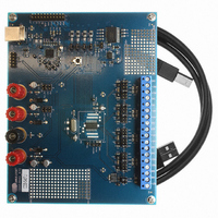
Manufacturer Part Number
CDB5467U
Description
BOARD EVAL FOR CS5467 ADC
Manufacturer
Cirrus Logic Inc
Type
A/Dr
Specifications of CDB5467U
Main Purpose
Power Management, Energy/Power Meter
Embedded
Yes, MCU, 8-Bit
Utilized Ic / Part
CS5467
Primary Attributes
Watt-Hour Meter
Secondary Attributes
Graphical User Interface, SPI™ & USB Interfaces
Product
Data Conversion Development Tools
Maximum Clock Frequency
4 MHz
Interface Type
USB
Supply Voltage (max)
5 V
Supply Voltage (min)
3.3 V
For Use With/related Products
CS5467
Lead Free Status / RoHS Status
Contains lead / RoHS non-compliant
Lead Free Status / RoHS Status
Lead free / RoHS Compliant, Contains lead / RoHS non-compliant
Other names
598-1555
CDB-5467U
CDB-5467U


7.6.5 Register Read and Write
DS714F1
B7
0
W/R
RA[4:0]
Page 0 Registers
Read and Write commands provide access to on-chip registers. After a Read command, the addressed data
can be clocked out the SDO pin by SCLK. After a Write command, 24 bits of write data must follow. The data
is transferred to the addressed register after the 24
of 32 addresses each. To access a desired page, write its number to the Page register at address 31.
Address
Warning: Do not write to unpublished register locations.
W/R
B6
0
1
2
3
4
5
6
7
8
9
10
11
12
13
14
15
16
17
18
19
20
21
22
23
24
25
26
27
28
29
30
31 R
31 W
RA4
B5
0 = Read
1 = Write
Write/Read control
Register address.
RA[4:0]
00000
00001
00010
00011
00100
00101
00110
00111
01000
01001
01010
01011
01100
01101
01110
01111
10000
10001
10010
10011
10100
10101
10110
10111
11000
11001
11010
11011
11100
11101
11110
11111
11111
RA3
B4
RA2
B3
Name
Config
I1
V1
P1
P1
I1
V1
I2
V2
P2
P2
I2
V2
Q1
Q1
Status
Q2
Q2
I1
V1
S1
PF1
I2
V2
S2
PF2
Mask
T
Ctrl
E
S
Q
Page
PULSE
PULSE
PULSE
RMS
RMS
PEAK
PEAK
AVG
RMS
AVG
RMS
PEAK
PEAK
AVG
AVG
RA1
B2
RA0
B1
Description
Configuration
Instantaneous Current Channel 1
Instantaneous Voltage Channel 1
Instantaneous Power Channel 1
Active Power Channel 1
RMS Current Channel 1
RMS Voltage Channel 1
Instantaneous Current Channel 2
Instantaneous Voltage Channel 2
Instantaneous Power Channel 2
Active Power Channel 2
RMS Current Channel 2
RMS Voltage Channel 2
Reactive Power Channel 1
Instantaneous Quadrature Power Channel 1
Internal Status
Reactive Power Channel 2
Instantaneous Quadrature Power Channel 2
Peak Current Channel 1
Peak Voltage Channel 1
Apparent Power Channel 1
Power Factor Channel 1
Peak Current Channel 2
Peak Voltage Channel 2
Apparent Power Channel 2
Power Factor Channel 2
Interrupt Mask
Temperature
Control
Active Energy Pulse Output
Apparent Energy Pulse Output
Reactive Energy Pulse Output
Register Page Select
B0
0
th
data bit is received. Registers are organized into pages
CS5467
27
Related parts for CDB5467U
Image
Part Number
Description
Manufacturer
Datasheet
Request
R

Part Number:
Description:
Development Kit
Manufacturer:
Cirrus Logic Inc
Datasheet:
Part Number:
Description:
Development Kit
Manufacturer:
Cirrus Logic Inc
Datasheet:


Part Number:
Description:
High-efficiency PFC + Fluorescent Lamp Driver Reference Design
Manufacturer:
Cirrus Logic Inc
Datasheet:
Part Number:
Description:
Development Kit
Manufacturer:
Cirrus Logic Inc
Datasheet:
Part Number:
Description:
Development Kit
Manufacturer:
Cirrus Logic Inc
Datasheet:

Part Number:
Description:
Development Kit
Manufacturer:
Cirrus Logic Inc
Datasheet:
Part Number:
Description:
Development Kit
Manufacturer:
Cirrus Logic Inc
Datasheet:
Part Number:
Description:
Development Kit
Manufacturer:
Cirrus Logic Inc
Datasheet:
Part Number:
Description:
Development Kit
Manufacturer:
Cirrus Logic Inc
Datasheet:

Part Number:
Description:
EVALUATION BOARD FOR CS8427
Manufacturer:
Cirrus Logic Inc
Datasheet:

Part Number:
Description:
BOARD EVAL FOR CS8416 RCVR
Manufacturer:
Cirrus Logic Inc
Datasheet:

Part Number:
Description:
EVALUATION BOARD FOR CS8420
Manufacturer:
Cirrus Logic Inc
Datasheet:

Part Number:
Description:
KIT DEVELOPMENT EP9315 ARM9
Manufacturer:
Cirrus Logic Inc
Datasheet:

Part Number:
Description:
KIT DEVELOPMENT EP9302 ARM9
Manufacturer:
Cirrus Logic Inc
Datasheet: