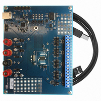
CDB5467U Cirrus Logic Inc, CDB5467U Datasheet - Page 4

CDB5467U
Manufacturer Part Number
CDB5467U
Description
BOARD EVAL FOR CS5467 ADC
Manufacturer
Cirrus Logic Inc
Type
A/Dr
Specifications of CDB5467U
Main Purpose
Power Management, Energy/Power Meter
Embedded
Yes, MCU, 8-Bit
Utilized Ic / Part
CS5467
Primary Attributes
Watt-Hour Meter
Secondary Attributes
Graphical User Interface, SPI™ & USB Interfaces
Product
Data Conversion Development Tools
Maximum Clock Frequency
4 MHz
Interface Type
USB
Supply Voltage (max)
5 V
Supply Voltage (min)
3.3 V
For Use With/related Products
CS5467
Lead Free Status / RoHS Status
Contains lead / RoHS non-compliant
Lead Free Status / RoHS Status
Lead free / RoHS Compliant, Contains lead / RoHS non-compliant
Other names
598-1555
CDB-5467U
CDB-5467U
1.3
The CDB5467U evaluation board provides screw-type terminals (J21, J23, J27, & J28) to connect input
signals to the voltage and current channels. The screw terminals are labels as VIN2-, VIN2+, VIN1-,
VIN1+, IIN1+, IIN1-, and IIN2+, IIN2-. An R-C network at each channel input provides a simple anti-alias
filter.
The evaluation board provides three voltage reference options for VREFIN to the CS5467. The three volt-
age reference options include: VREFOUT from CS5467, the on-board +2.5V reference, and external
REF+ (screw terminal J14).
on J25 in the position labeled VREFOUT, the reference is supplied by the on-chip voltage reference. With
a jumper on J25 in the position labeled VREF, the reference is supplied by an off-chip voltage reference.
Table 2
provides a +2.5V reference (the LT1019 was chosen for its low drift - typically 5 ppm/°C). By setting the
jumper on J12 to position REF+, an external voltage reference is supplied via screw terminal J14's REF+
input.
The three input signal options for the voltage (VIN1±, VIN2±) and current (IIN1±, IIN2±) channels input
include: an external signal (screw terminals J21, J23, J27, and J28), GND, or VREF. Table3 illustrates the
options available. By installing jumpers on J11 to position VIN2-, J7 to position VIN2+, J17 to position
VIN1-, J22 to position VIN1+, J24 to position IIN1+, J26 to position IIN1-, J20 to position IIN2+, and J19
to position IIN2-, the input voltage signal is supplied from the screw terminals J21, J23, J27, and J28. With
a jumper on J11, J7, J17, J22, J24, J26, J20 and J19 in the GND position, the inputs are connected to
4
Analog Section
illustrates the options available for VREF. With a jumper on J12 in position LT1019, the LT1019
Table 2. External Voltage Reference Selection for VREF
Table 1. Internal Voltage Reference Selection for VREF
Table 1
Reference
Reference
VREFOUT
LT1019
REF+
VREF
and
Table 2
LT1019 Reference
Reference Source
Selects On-board
Selects External
LT1019 Reference(J12)
Reference (25 ppm/
Description
(5 ppm/
Selects External or
Selects On-chip
(J14)
Description
illustrate the options available for VREFIN. With a jumper
°
C)
LT1019
LT1019
°
REF+
REF+
C)
O
O
(Default)
J12
VREFOUT
VREFOUT
VREFIN
VREFIN
(Default)
O
O
O
O
J25
VREF
VREF
VREF
VREF
VREF
VREF
O
O
O
O
CDB5467U
DS714DB1


