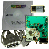
EVAL-ADF4118EBZ1 Analog Devices Inc, EVAL-ADF4118EBZ1 Datasheet - Page 6
EVAL-ADF4118EBZ1
Manufacturer Part Number
EVAL-ADF4118EBZ1
Description
BOARD EVAL FOR ADF4118
Manufacturer
Analog Devices Inc
Datasheet
1.ADF4116BRUZ-REEL.pdf
(28 pages)
Specifications of EVAL-ADF4118EBZ1
Main Purpose
Timing, Frequency Synthesizer
Embedded
No
Utilized Ic / Part
ADF4118
Primary Attributes
Single Integer-N PLL
Secondary Attributes
1.96GHz WCDMA, Graphical User Interface
Lead Free Status / RoHS Status
Lead free / RoHS Compliant


ADF4116/ADF4117/ADF4118
ABSOLUTE MAXIMUM RATINGS
T
Table 3.
Parameter
AV
AV
V
V
Digital I/O Voltage to GND
Analog I/O Voltage to GND
REF
RF
Operating Temperature Range
Storage Temperature Range
Maximum Junction Temperature
TSSOP θ
Reflow Soldering
Transistor Count
1
GND = AGND = DGND = 0 V.
P
P
A
Industrial (B Version)
Extended (Y Version)
Peak Temperature
Time at Peak Temperature
CMOS
Bipolar
IN
DD
DD
to GND
to AV
= 25°C, unless otherwise noted.
IN
A to RF
, RF
to GND
to DV
DD
JA
IN
A, RF
1
Thermal Impedance
DD
IN
B
1
IN
B to GND
1
1
1
Rating
−0.3 V to +7 V
−0.3 V to +0.3 V
−0.3 V to +7 V
−0.3 V to +5.5 V
−0.3 V to V
−0.3 V to V
−0.3 V to V
±320 mV
−40°C to +85°C
−40°C to +125°C
−65°C to +150°C
150°C
112°C/W
260°C
40 sec
6425
303
DD
P
DD
+ 0.3 V
+ 0.3 V
+ 0.3 V
Rev. D | Page 6 of 28
Stresses above those listed under Absolute Maximum Ratings
may cause permanent damage to the device. This is a stress
rating only; functional operation of the device at these or any
other conditions above those indicated in the operational
section of this specification is not implied. Exposure to absolute
maximum rating conditions for extended periods may affect
device reliability.
This device is a high performance RF integrated circuit with an
ESD rating of <2 kV, and it is ESD sensitive. Proper precautions
should be taken for handling and assembly.
ESD CAUTION
Related parts for EVAL-ADF4118EBZ1
Image
Part Number
Description
Manufacturer
Datasheet
Request
R

Part Number:
Description:
IC, ADJ LDO REG, 1.5V TO 5V 250mA MSOP-8
Manufacturer:
Vishay
Datasheet:

Part Number:
Description:
IC, ADJ LDO REG, 1.5V TO 5V 0.6A 8-TSSOP
Manufacturer:
Vishay
Datasheet:
Part Number:
Description:
IC, ADJ LDO REG, 1.5V TO 5V 250mA MSOP-8
Manufacturer:
Vishay
Datasheet:

Part Number:
Description:
IC ADJ LDO REG 1.5V TO 5V 150mA 5-SOT-23
Manufacturer:
Vishay
Datasheet:

Part Number:
Description:
BOARD EVAL AS1324-AD
Manufacturer:
austriamicrosystems
Datasheet:
Part Number:
Description:
IC, ADJ LDO REG, 1.5V TO 5V 0.6A 8-TSSOP
Manufacturer:
Vishay
Datasheet:

Part Number:
Description:
IC, ADJ LDO REG, 1.5V TO 5V, 0.3A, MSOP8
Manufacturer:
Vishay
Datasheet:
Part Number:
Description:
IC, ADJ LDO REG, 1.5V TO 5V, 0.3A, MSOP8
Manufacturer:
Vishay
Datasheet:
Part Number:
Description:
IC, ADJ LDO REG 1.215V TO 5V 0.3A MSOP-8
Manufacturer:
Vishay
Datasheet:
Part Number:
Description:
IC, ADJ LDO REG 1.215V TO 5V 0.3A MSOP-8
Manufacturer:
Vishay
Datasheet:

Part Number:
Description:
±1.7g Dual-Axis IMEMS Accelerometer Evaluation Board
Manufacturer:
Analog Devices Inc
Datasheet:

Part Number:
Description:
IC MULTIPLIER ANALOG 8-SOIC T/R
Manufacturer:
Analog Devices Inc
Datasheet:

Part Number:
Description:
IC ANALOG MULTIPLIER 8-DIP
Manufacturer:
Analog Devices Inc
Datasheet:
Part Number:
Description:
IC ANALOG MULTIPLIER 8-SOIC
Manufacturer:
Analog Devices Inc
Datasheet:
Part Number:
Description:
IC ANALOG MULTIPLIER 8-DIP
Manufacturer:
Analog Devices Inc
Datasheet: