AD5162EVAL Analog Devices Inc, AD5162EVAL Datasheet - Page 6
AD5162EVAL
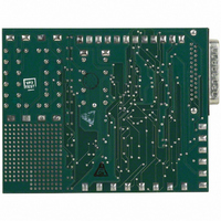
Manufacturer Part Number
AD5162EVAL
Description
BOARD EVAL FOR AD5162
Manufacturer
Analog Devices Inc
Datasheet
1.AD5162BRMZ2.5.pdf
(20 pages)
Specifications of AD5162EVAL
Main Purpose
Digital Potentiometer
Utilized Ic / Part
AD5162
Lead Free Status / RoHS Status
Contains lead / RoHS non-compliant
Secondary Attributes
-
Embedded
-
Primary Attributes
-


AD5162
ABSOLUTE MAXIMUM RATINGS
T
Table 4.
Parameter
V
V
Terminal Current, Ax to Bx, Ax to Wx, Bx to Wx
Digital Inputs and Output Voltage to GND
Operating Temperature Range
Maximum Junction Temperature (T
Storage Temperature
Lead Temperature (Soldering, 10 sec)
Thermal Resistance, θ
1
2
The maximum terminal current is bound by the maximum current handling
of the switches, the maximum power dissipation of the package, and the
maximum applied voltage across any two of the A, B, and W terminals at a
given resistance.
The package power dissipation is (T
DD
A
A
, V
Pulsed
Continuous
= 25°C, unless otherwise noted.
to GND
B
, V
W
to GND
JA
for 10-Lead MSOP
JMAX
− T
JMAX
A
)/θ
)
JA
.
2
1
Rating
–0.3 V to +7 V
V
±20 mA
±5 mA
0 V to 7 V
–40°C to +125°C
150°C
–65°C to +150°C
300°C
230°C/W
DD
Rev. C | Page 6 of 20
Stresses above those listed under Absolute Maximum Ratings
may cause permanent damage to the device. This is a stress
rating only; functional operation of the device at these or any
other conditions above those indicated in the operational
section of this specification is not implied. Exposure to absolute
maximum rating conditions for extended periods may affect
device reliability.
ESD CAUTION
Related parts for AD5162EVAL
Image
Part Number
Description
Manufacturer
Datasheet
Request
R


Part Number:
Description:
Board Mount Temperature Sensors TEMP MONITR DUAL CHN W/SERIES RSTNCE CNCL
Manufacturer:
ON Semiconductor
Datasheet:

Part Number:
Description:
Touch Screen Digitizer
Manufacturer:
Analog Devices, Inc.
Datasheet:
Part Number:
Description:
Half-duplex Icoupler-r Isolated Rs-485 Transceiver
Manufacturer:
Analog Devices, Inc.
Datasheet:

Part Number:
Description:
±1.7g Dual-Axis IMEMS Accelerometer Evaluation Board
Manufacturer:
Analog Devices Inc
Datasheet:

Part Number:
Description:
Inertial Sensor Evaluation System
Manufacturer:
Analog Devices Inc
Datasheet:
Part Number:
Description:
Manufacturer:
Analog Devices Inc
Datasheet:
Part Number:
Description:
Manufacturer:
Analog Devices Inc
Datasheet:
Part Number:
Description:
Manufacturer:
Analog Devices Inc
Datasheet:
Part Number:
Description:
Manufacturer:
Analog Devices Inc
Datasheet:
Part Number:
Description:
Manufacturer:
Analog Devices Inc
Datasheet: