ATA6623-EK Atmel, ATA6623-EK Datasheet - Page 3
ATA6623-EK
Manufacturer Part Number
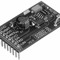
ATA6623-EK
Description
BOARD DEMO LIN SBC FOR ATA6623
Manufacturer
Atmel
Specifications of ATA6623-EK
Main Purpose
Interface, LIN
Embedded
Yes, MCU, 8-Bit
Utilized Ic / Part
ATA6623
Primary Attributes
LIN-SBC (System-Basis-Chip) Transceiver, LIN 2.0, Voltage Regulator
Secondary Attributes
4 Power Modes: Pre-Normal, Normal, Sleep, Silent, 8-SOIC
Lead Free Status / RoHS Status
Contains lead / RoHS non-compliant


2.3
2.3.1
2.3.2
2.3.3
2.4
4969B–AUTO–03/11
LIN Interface (LIN, TXD and RXD)
Undervoltage Reset Output (NRES)
Bus Pin (LIN)
Input Pin (TXD)
Output Pin (RXD)
A low-side driver with internal current limitation and thermal shutdown and an internal pull-up
resistor in compliance with the LIN specification 2.0 is implemented. LIN receiver thresholds
are compatible with the LIN protocol specification.
At the LIN pin there is a 220-pF capacitor to ground on the board. There is the possibility of
additionally mounting the two extra components diode D2 (LL4148) in series with resistor R1
(1k ) on the board at their designated placeholders, necessary when using the development
board for a LIN master application.
This pin is the microcontroller interface to control the state of the LIN output. TXD must be
pulled to ground in order to have the LIN bus low. If TXD is high, the LIN output transistor is
turned off and the bus is in the recessive state, pulled up by the internal resistor. If TXD is low,
the LIN output transistor is turned on and the bus is in the dominant state. An internal timer
prevents the bus line from being driven permanently in the dominant state. If TXD is forced to
low longer than t
This pin reports the state of the LIN bus to the microcontroller. LIN high (recessive state) is
reported by a high level at RXD, LIN low (dominant state) is reported by a low level at RXD.
The output has an internal pull-up structure with typ. 5k resistance to VCC and is short circuit
protected.
In the Atmel
the VCC voltage falls below the undervoltage threshold, NRES switches to LOW after a
debounce time of approximately 2µs. The implemented undervoltage delay keeps NRES at a
low level for approximately 10ms after VCC reaches its nominal value.
In the Atmel ATA6623 and Atmel ATA6625, the Reset output is an open-drain output imple-
mented using a single MOS transistor which is switched on in the case of a VCC undervoltage.
In order to pull up the output of the Atmel ATA6623/25, an external resistor connected to VCC
is necessary. Space for this resistor (R2) is available on the development board .
If a reset occurs (NRES is low), the circuit switches to pre-normal mode.
®
ATA6620, the Reset output is a push-pull stage supplied by the VCC voltage. If
DOM
> 20 ms, the LIN bus driver is switched to the recessive state.
Atmel ATA6620/23/25
3
Related parts for ATA6623-EK
Image
Part Number
Description
Manufacturer
Datasheet
Request
R

Part Number:
Description:
TXRX LIN BUS W/VREG 3.3V SO-8
Manufacturer:
Atmel
Datasheet:
Part Number:
Description:
TXRX LIN BUS W/VREG 3.3V SO-8
Manufacturer:
Atmel
Datasheet:

Part Number:
Description:
LIN Bus Transceiver with 3.3V Voltage Regulator
Manufacturer:
ATMEL Corporation
Datasheet:
Part Number:
Description:
(ATA6623 / ATA6625) LIN Bus Transceiver
Manufacturer:
ATMEL Corporation
Datasheet:

Part Number:
Description:
DEV KIT FOR AVR/AVR32
Manufacturer:
Atmel
Datasheet:
Part Number:
Description:
INTERVAL AND WIPE/WASH WIPER CONTROL IC WITH DELAY
Manufacturer:
ATMEL Corporation
Datasheet:
Part Number:
Description:
Low-Voltage Voice-Switched IC for Hands-Free Operation
Manufacturer:
ATMEL Corporation
Datasheet:
Part Number:
Description:
MONOLITHIC INTEGRATED FEATUREPHONE CIRCUIT
Manufacturer:
ATMEL Corporation
Datasheet:
Part Number:
Description:
AM-FM Receiver IC U4255BM-M
Manufacturer:
ATMEL Corporation
Datasheet:
Part Number:
Description:
Monolithic Integrated Feature Phone Circuit
Manufacturer:
ATMEL Corporation
Datasheet:
Part Number:
Description:
Multistandard Video-IF and Quasi Parallel Sound Processing
Manufacturer:
ATMEL Corporation
Datasheet:
Part Number:
Description:
High-performance EE PLD
Manufacturer:
ATMEL Corporation
Datasheet: