NBC124XXEVB ON Semiconductor, NBC124XXEVB Datasheet - Page 14
NBC124XXEVB
Manufacturer Part Number
NBC124XXEVB
Description
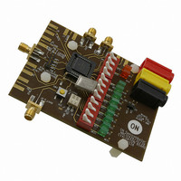
EVAL BOARD FOR NBC124XX
Manufacturer
ON Semiconductor
Datasheets
1.NBC12439FAR2G.pdf
(21 pages)
2.NBC12429FAR2G.pdf
(22 pages)
3.NBC12430FAR2G.pdf
(20 pages)
Specifications of NBC124XXEVB
Design Resources
NBC124XXEVB Gerber Files
Main Purpose
Timing, PLL
Embedded
No
Utilized Ic / Part
NBC12429, NBC12430, NBC12439
Primary Attributes
DIP Switch Controlled M & N Logic
Secondary Attributes
Push Button or Externally Controlled P_Load
Technology Type
Evaluation Board
Lead Free Status / RoHS Status
Lead free / RoHS Compliant
For Use With/related Products
NBC124XX
Other names
NBC124XXEVBOS


application dependent but the JEDEC specification is 1000
cycles. See Figure 11.
the highest and lowest acquired value and is represented as
the width of the Gaussian base. See Figure 12.
are confused with one another. An earlier method of
measuring jitter is to look at the timing signal with an
oscilloscope and observe the variations in period−to−period
or cycle−to−cycle. If the scope is set up to trigger on every
rising or falling edge, set to infinite persistence mode and
allowed to trace sufficient cycles, it is possible to determine
the maximum and minimum periods of the timing signal.
Digital scopes can accumulate a large number of cycles,
create a histogram of the edge placements and record
peak−to−peak as well as standard deviations of the jitter.
Care must be taken that the measured edge is the edge
immediately following the trigger edge. These scopes can
also store a finite number of period durations and
post−processing software can analyze the data to find the
maximum and minimum periods.
Random Peak−to−Peak Jitter is the difference between
There are different ways to measure jitter and often they
Figure 12. Random Peak−to−Peak and RMS Jitter
*1,000 − 10,000 Cycles
Figure 11. Cycle−to−Cycle Jitter
T
0
Time*
T
JITTER(cycle−cycle)
= T
T
1
1
− T
Typical
Gaussian
Distribution
0
RMS
or one
Sigma
Jitter
http://onsemi.com
14
resulted in advanced jitter measurement techniques. The
Tektronix TDS−series oscilloscopes have superb jitter
analysis capabilities on non−contiguous clocks with their
histogram and statistics capabilities. The Tektronix
TDSJIT2/3 Jitter Analysis software provides many key
timing parameter measurements and will extend that
capability by making jitter measurements on contiguous
clock and data cycles from single−shot acquisitions.
correlated.
and are more accurate. All of the jitter data reported on the
NBC12439 and NBC12439A was collected in this manner.
Figure 13 shows the RMS jitter performance as a function
of the VCO frequency range. The general trend is that as the
VCO frequency is increased, the RMS output jitter will
decrease.
the output frequency. Note the jitter is a function of both the
output frequency as well as the VCO frequency. However,
the VCO frequency shows a much stronger dependence.
observed at the end of a period’s edge when compared to the
position of the perfect reference clock’s edge and is
specified by the number of cycles over which the jitter is
measured. The number of cycles used to look for the
maximum jitter varies by application but the JEDEC spec is
10,000 observed cycles.
cycle−to−cycle jitter, which rivals that of SAW based
oscillators. This jitter performance comes with the added
flexibility associated with a synthesizer over a fixed
frequency oscillator. The jitter data presented should
provide users with enough information to determine the
effect on their overall timing budget. The jitter performance
meets the needs of most system designs while adding the
flexibility of frequency margining and field upgrades. These
features are not available with a fixed frequency SAW
oscillator.
Recent hardware and software developments have
M1 by Amherst was used as well and both test methods
This test process can be correlated to earlier test methods
Figure 14 illustrates the RMS jitter performance versus
Long−Term Period Jitter is the maximum jitter
The NBC12439 and NBC12439A exhibit long term and
Related parts for NBC124XXEVB
Image
Part Number
Description
Manufacturer
Datasheet
Request
R

Part Number:
Description:
ON Semiconductor [VOLTAGE REGULATOR]
Manufacturer:
ON Semiconductor
Datasheet:
Part Number:
Description:
357-036-542-201 CARDEDGE 36POS DL .156 BLK LOPRO
Manufacturer:
ON Semiconductor
Datasheet:
Part Number:
Description:
357-036-542-201 CARDEDGE 36POS DL .156 BLK LOPRO
Manufacturer:
ON Semiconductor
Datasheet:
Part Number:
Description:
357-036-542-201 CARDEDGE 36POS DL .156 BLK LOPRO
Manufacturer:
ON Semiconductor
Datasheet:
Part Number:
Description:
357-036-542-201 CARDEDGE 36POS DL .156 BLK LOPRO
Manufacturer:
ON Semiconductor
Datasheet:
Part Number:
Description:
357-036-542-201 CARDEDGE 36POS DL .156 BLK LOPRO
Manufacturer:
ON Semiconductor
Datasheet:
Part Number:
Description:
357-036-542-201 CARDEDGE 36POS DL .156 BLK LOPRO
Manufacturer:
ON Semiconductor
Datasheet:
Part Number:
Description:
357-036-542-201 CARDEDGE 36POS DL .156 BLK LOPRO
Manufacturer:
ON Semiconductor
Datasheet:
Part Number:
Description:
357-036-542-201 CARDEDGE 36POS DL .156 BLK LOPRO
Manufacturer:
ON Semiconductor
Datasheet:
Part Number:
Description:
357-036-542-201 CARDEDGE 36POS DL .156 BLK LOPRO
Manufacturer:
ON Semiconductor
Datasheet:
Part Number:
Description:
357-036-542-201 CARDEDGE 36POS DL .156 BLK LOPRO
Manufacturer:
ON Semiconductor
Datasheet:
Part Number:
Description:
Manufacturer:
ON Semiconductor
Datasheet:
Part Number:
Description:
Manufacturer:
ON Semiconductor
Datasheet:
Part Number:
Description:
Manufacturer:
ON Semiconductor
Datasheet: