DEMOBOARD TLE8201R Infineon Technologies, DEMOBOARD TLE8201R Datasheet - Page 22
DEMOBOARD TLE8201R
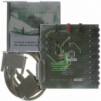
Manufacturer Part Number
DEMOBOARD TLE8201R
Description
BOARD DEMO TLE8201R V1.0
Manufacturer
Infineon Technologies
Datasheet
1.TLE8201R.pdf
(45 pages)
Specifications of DEMOBOARD TLE8201R
Main Purpose
Power Management, High & Low Side Driver (Internal FET)
Embedded
No
Utilized Ic / Part
TLE8201
Primary Attributes
1 H-Bridge @ 3A, 4 Half Bridges- 2 @ 1A, 2 @ 0.5A, 5 High Side 1@ 2.5A, 4 @ 0..5A
Secondary Attributes
SPI Interface, Intended for Automotive Door
Lead Free Status / RoHS Status
Lead free / RoHS Compliant
Other names
DEMOBOARDTLE8201RIN


Electrical Characteristics - SPI-timing
8 V <
-40 C <
Pos. Parameter
4.3.5 DI data setup time
4.3.6 DI data hold time
4.3.7 DI data valid time
4.3.8 DO data setup time
4.3.9 DO data hold time
4.3.10 No-data-time between SPI
4.3.11 Clock frequency
4.3.12 Duty cycle of incoming
1)
Figure 7
4.3.6
The PWM inputs PWM1 and PWM2 are direct power stage control inputs that can be
used to switch on and off one or more of the power transistors with a PWM signal
supplied to this pin. The setting of the SPI Registers CtrlReg_01 and CtrlReg_11 defines
which of the power stages will be controlled by the PWM inputs. If the selection-bits of
Data Sheet Rev. 2.0
CSN
CLK
DO
SPI Timing is not subject to production test - specified by design. SPI functional test is performed at 5 MHz CLK
frequency. Timing specified with an external load of 30pF at pin [DO].
DI
V
commands
clock at CLK
S
T
< 20 V; 4.75 V <
j
< 150 C; unless otherwise specified
1
PWM inputs
Timing Diagram
not defined
8
1
Flag
V
CC
4
7
< 5.25 V; INH = High; all outputs open;
MSB
MSB
Sym-
bol
t
t
t
t
t
t
f
–
5
SU
h
v
DOsetup
DOhold
nodata
CL
22
3
6
min. typ.
40
40
–
0
50
5
–
40
Limit Values
–
–
–
–
–
–
–
–
max.
–
–
50
60
–
–
2
60
LSB
LSB
Unit Conditions
ns
ns
ns
ns
ns
MHz
%
2
s
5
6
–
7 and 8
9
10
1)
–
1)
1)
1)
1)
1)
9
TLE 8201R
1)
2
2006-06-07
10
1)
Related parts for DEMOBOARD TLE8201R
Image
Part Number
Description
Manufacturer
Datasheet
Request
R

Part Number:
Description:
BOARD DEMO FOR TLE6208-3G
Manufacturer:
Infineon Technologies
Datasheet:

Part Number:
Description:
BOARD DEMO FOR TLE6208-6G
Manufacturer:
Infineon Technologies
Datasheet:

Part Number:
Description:
BOARD DEMO FOR TLE 6288R
Manufacturer:
Infineon Technologies
Datasheet:

Part Number:
Description:
BOARD DEMO FOR TLE 6214L
Manufacturer:
Infineon Technologies
Datasheet:

Part Number:
Description:
BOARD DEMO FOR TLE 7209-2R
Manufacturer:
Infineon Technologies
Datasheet:

Part Number:
Description:
BOARD DEMO PROFET V2.0BTS
Manufacturer:
Infineon Technologies
Datasheet:

Part Number:
Description:
BOARD DEMO FOR TLE 6244X
Manufacturer:
Infineon Technologies
Datasheet:

Part Number:
Description:
BOARD DEMO FOR TLE 6365 REV.4
Manufacturer:
Infineon Technologies
Datasheet:

Part Number:
Description:
BOARD DEMO FOR TLE 6389-2GV
Manufacturer:
Infineon Technologies
Datasheet:

Part Number:
Description:
BOARD DEMO FOR TLE 6389-2 GV50
Manufacturer:
Infineon Technologies
Datasheet:

Part Number:
Description:
Manufacturer:
Infineon Technologies AG
Datasheet:
Part Number:
Description:
Manufacturer:
Infineon Technologies AG
Datasheet:
Part Number:
Description:
Manufacturer:
Infineon Technologies AG
Datasheet:
Part Number:
Description:
Manufacturer:
Infineon Technologies AG
Datasheet:
Part Number:
Description:
Manufacturer:
Infineon Technologies AG
Datasheet: