W6810DK Nuvoton Technology Corporation of America, W6810DK Datasheet
W6810DK
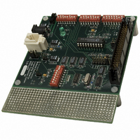
Specifications of W6810DK


Related parts for W6810DK

W6810DK Summary of contents
Page 1
Winbond W6810, W681310 W681360, W681512, W681513 and CODEC Evaluation System W681xxx DK Evaluation Board WECA 2727 N First Street, San Jose CA 95134 W6811 User’s Guide Rev 6.12 1 W681xxxDK ...
Page 2
Chapter - 1 Products supported by the W681xxx DK: Part # of PCM Supply Number Channels Format Voltage 1 -Law / W6810 A-Law 1 -Law / 5V Analog W6811 A-Law 3V Digital 1 -Law / W681310 A-Law 1 13-bit W681360 ...
Page 3
W6810 Features • Single +5 VDC power supply • Typical power dissipation of 25 mW, power-down mode of 0.5 µW • Fully-differential analog circuit design • On-chip precision reference of 1.575 V for a 0 dBm 0TLP at 600Ω. • ...
Page 4
W681310 Features • Single +3 VDC power supply • Typical power dissipation of 25 mW, power-down mode of 0.5 µW • Fully-differential analog circuit design • On-chip precision reference of 1.575 V for a -5.0 dBm 0TLP at 600Ω. • ...
Page 5
General Description Winbond’s W681XXXDK Evaluation/Development System is a Stand-Alone unit that serves as a simple, easy-to-use demonstration board as well as a powerful evaluation system. All the functions of the W6810/W681310/ W681360 PCM CODECs may be selected in real time ...
Page 6
W681xxxDK Features: Easy to use (a stand-alone evaluation system) • Single +5 VDC power supply ( not supplied) • Single +3 VDC Power Supply ( not supplied) for W6811 or W681310/W681360 • Prototype area for application development • Useful connectors ...
Page 7
Chapter - 2 Hardware Description Clock Generator: All the necessary clock rates such as Frame Sync, Bit Clock and the 256 KHz for the W681xxxDK evaluation system are driven from a single 4.096 MHz crystal oscillator. Frame Sync: The Frame ...
Page 8
Frame Sync = 3 BCLK ON OFF Frame Sync = 1 ON OFF 1 BIT CLOCK: Bit clock is routed to the 2x20 (J11) header connector pins 5 (BCLKT) and 36 (BCLKR) through J17A and J14 used to ...
Page 9
Figure 2: W681xxxDK Evaluation System Schematic Diagram VCC 100 1uF J5 C14 68uF .1uF J6 R10 200K MIC+ A Handset DIP MIC ...
Page 10
U1D 74HCU04/SO U1E U4A CLK R1 2 CLR 100 R2 74HC393/SO 10M Y1 U4B 13 CLK 4.096MHz 12 CLR C1 22pF C2 22pF 74HC393/SO U1F 74HCU04/ PWR OFF/ON SW1 EG1903-ND C3 68uF ...
Page 11
... When a Jumper is populated (switch is Closed), it enables the function; an unpopulated Jumper (Open Switch) disables the function. The Jumpers are referenced as letters; for example J7A, J7B. Only one Jumper is closed for a selected function, not both, or the power supply can be shorted! W6810DK JUMPERS/DIP SWITCHES FOR W6810 DIP SWITCH JUMPER NUMBERS ...
Page 12
... W6810DK JUMPERS/DIP SWITCHES FOR W681360 LINEAR CODEC DIP SWITCH JUMPER NUMBERS NAME SW3-1 J2A -2 J2B -3 N/U -4 N J9A -8 J9B SW4 J10A -3 J10B -4 J12A -5 J12B -6 J13 -7 J15A -8 J15B SW5-1 J14 -2 JI6A -3 J16B -4 J18 -5 J19A -6 J19B -7 J19C -8 J20 J17A J17B J17C J1 WARNING: Jumpers shaded can short Vcc to Ground if set wrong. ...
Page 13
W681512DK JUMPERS/DIP SWITCHES FOR A-A, A-D, D-A TESTING DIP SWITCH JUMPER NUMBERS NAME SW3-1 J2A -2 J2B -3 N/U -4 N J9A -8 J9B SW4 J10A -3 J10B -4 J12A -5 J12B -6 ...
Page 14
PCM-4 General Parameter Settings Parameter # Selected 1 11 14, 24 13 11, 12, 22 (11, 21 11, 13, 16, 22, 23, 27, ...
Page 15
J3: Power Supply Input Jack (5VDC or 3VDC) If you are evaluating a 5V product use 5VDC power supply. If you are evaluating a 3V product use a 3VDC power supply adapter with positive center. J4: GND TST points J5: ...
Page 16
J13: PCMT: (SW4-6) J13 Connects the PCMT (PCM output W681xxx) to J11 (Pin 9). J14: BCLKT=BCLK (SW5-1) J14 connects BCLK to BCLKT (Pin 12) of the W6810/W681310 CODEC-Filter. J15A: MCLK = 256 KHz (SW4-7) J15A sets the MCLK (Pin 11) ...
Page 17
J19C: FSR = GND (SW5-7) SELECT B1 IN GCI ISDN MODE J19C connects FSR (Pin 7) of the W6810/W681310 CODEC to Ground. J20: FSX= FSYNC (SW5-8) J20 connects the on board generated Frame Sync to W6810/W681310 FSX (Pin 14) as ...
Page 18
Chapter - 4 Operation Modes The W681xxx-DK operates in two modes, Standalone and Back-To-Back mode. Standalone Operation: In this mode of operation the analog signal input at Transmit input (J7), is presented to the encoder of the W6810/W681310/W681360, where it ...
Page 19
... Note: Do not connect the power supply to the second board. It will be bussed to the second board through the 2x20 cable. Make sure the cable is connected as shown below. J17 = Open WECA 2727 N First Street, San Jose CA 95134 Slave Board 2 W6810DK JUMPERS/DIP SWITCHES Master 0 1 Board 1 19 W681xxxDK ...
Page 20
FOR W6810 BACK-TO-BACK TEST DIP JUMPER SWITCH NAME NUMBERS SW3-1 J2A 16 KHz Sync N/C -2 J2B -3 N/U -4 N J9A -8 J9B SW4 J10A -3 J10B -4 J12A -5 J12B -6 ...
Page 21
W6810/W681310 Conversion to W6811 The W6811 is a general-purpose single channel PCM CODEC with pin-selectable µ-Law or A-Law companding. The device is compliant with the ITU G.712 specification. It operates from separate analog (5V) and digital (3V) power supplies. performed ...
Page 22
Vref VAG 2 19 RO- AI PAI AI PAO PAO+ U VDD VSS 7 14 FSR FST 8 13 PCMR PCMT 9 12 BCLKR BCLKT 10 11 PUI ...
Page 23
... W6810/W681310 Conversion to W681513 The W6810DK has to be modified to allow the demonstration of the W681513 because of the 2.000 MHz clock rather than the 2.048 MHz standard frequency. The W681xxx- DK board is designed to divide 2048 KHz by 256 to get the 8 KHz sample clock. For the W681513 we substitute a 4.000 MHz crystal on the board and then build an external divider to do the divide by 250 to get 8 KHz again ...
Page 24
U1D 74HCU04/SO U1E U4A CLK R1 2 CLR 100 R2 74HC393/SO 10M Y1 U4B 13 CLK 4.000MHz 12 CLR C1 22pF C2 22pF 74HC393/SO U1F 74HCU04/ PWR OFF/ON D2 SW1 EG1903-ND 1N5341 ...
Page 25
VCC R11 C17 R12 1K R10 100 1uF J5 3.9K C14 C13 R8 J5 C16 68uF .1uF 1uF 20K R9 J6 200K C15 .01uF J13 J9 1 MIC+ A U14 Vref VAG 4 SW DIP 2 ...
Page 26
Evaluation Board part Number Winbond CODEC Part number W6810 DK W681512DK W681310DK W681360DK W681xxxDK Part Number The information contained in this datasheet may be subject to change without notice the responsibility of the customer to check the Winbond ...