AD9516-1/PCBZ Analog Devices Inc, AD9516-1/PCBZ Datasheet - Page 11
AD9516-1/PCBZ
Manufacturer Part Number
AD9516-1/PCBZ
Description
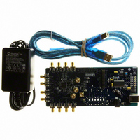
BOARD EVALUATION FOR AD9516-1
Manufacturer
Analog Devices Inc
Specifications of AD9516-1/PCBZ
Main Purpose
Timing, Clock Generator
Embedded
No
Utilized Ic / Part
AD9516-1
Primary Attributes
2 Inputs, 14 Outputs, 2.5GHz VCO
Secondary Attributes
CMOS, LVDS, LVPECL Output Logic, ADIsimCLK™ Graphical User Interface
Silicon Manufacturer
Analog Devices
Application Sub Type
PLL Clock Synthesizer
Kit Application Type
Clock & Timing
Silicon Core Number
AD9516-0, AD9516-1, AD9516-2
Silicon Family Name
AD9516-X
Rohs Compliant
Yes
Lead Free Status / RoHS Status
Lead free / RoHS Compliant


Evaluation Board User Guide
CHANNEL DIVIDER WINDOW
The channel divider window shown in Figure 18 is accessed by
clicking the appropriate channel divider. It is usually sufficient
to change only the divide ratio because the evaluation software
and the AD951x duty cycle correction ensure that the output
duty cycle remains very close to 50%.
You can also vary the phase offset by changing the Phase Offset
Bits setting. However, to have the new phase take effect, the
SYNC signal needs to be toggled by using the SYNC button
in the lower left corner of the main window.
Figure 18. Divider 1 Settings Window
Rev. 0 | Page 11 of 16
LVPECL OUTPUT DRIVER WINDOW
The LVPECL Output 0 Settings window shown in Figure 20 is
accessed by clicking the OUT0 through OUT5 output driver
symbols on the right side of the main window (see Figure 19).
It is important to power down unused outputs on the evaluation
board because they can be a source of unwanted spurs.
Figure 19. OUT0 Through OUT5 Output Driver Symbols
Figure 20. LVPECL Output 0 Driver Window
UG-075
Related parts for AD9516-1/PCBZ
Image
Part Number
Description
Manufacturer
Datasheet
Request
R

Part Number:
Description:
IC CLOCK PLL/VCO 2GHZ 64LFCSP
Manufacturer:
Analog Devices Inc
Datasheet:
Part Number:
Description:
IC CLOCK GEN 2.8GHZ VCO 64-LFCSP
Manufacturer:
Analog Devices Inc
Datasheet:
Part Number:
Description:
IC,Fourteen Distributed-Output Clock Driver,LLCC,64PIN,PLASTIC
Manufacturer:
Analog Devices Inc
Datasheet:
Part Number:
Description:
IC,Ten Distributed-Output Clock Driver,LLCC,64PIN,PLASTIC
Manufacturer:
Analog Devices Inc
Datasheet:
Part Number:
Description:
IC,Ten Distributed-Output Clock Driver,LLCC,64PIN,PLASTIC
Manufacturer:
Analog Devices Inc
Datasheet:
Part Number:
Description:
Clock IC With 1.8GHz On-chip VCO
Manufacturer:
Analog Devices Inc
Datasheet:

Part Number:
Description:
BOARD EVAL FOR AD9516-3 2.0GHZ
Manufacturer:
Analog Devices Inc
Datasheet:

Part Number:
Description:
BOARD EVAL FOR AD9516-4 1.8GHZ
Manufacturer:
Analog Devices Inc
Datasheet:
Part Number:
Description:
IC,Ten Distributed-Output Clock Driver,LLCC,64PIN,PLASTIC
Manufacturer:
Analog Devices Inc
Datasheet:
Part Number:
Description:
IC,Fourteen Distributed-Output Clock Driver,LLCC,64PIN,PLASTIC
Manufacturer:
Analog Devices Inc
Datasheet:
Part Number:
Description:
IC,Ten Distributed-Output Clock Driver,LLCC,64PIN,PLASTIC
Manufacturer:
Analog Devices Inc
Datasheet:
Part Number:
Description:
Clock IC With 1.8GHz On-chip VCO
Manufacturer:
Analog Devices Inc
Datasheet:
Part Number:
Description:
10/14 Chan Clock IC W/PLL-no VCO
Manufacturer:
Analog Devices Inc
Datasheet:
Part Number:
Description:
10/14 Chan Clock IC W/PLL-no VCO
Manufacturer:
Analog Devices Inc
Datasheet:

Part Number:
Description:
Clock IC With 2.5GHz On-chip VCO EB
Manufacturer:
Analog Devices Inc
Datasheet: