EVAL-AD2S1210EDZ Analog Devices Inc, EVAL-AD2S1210EDZ Datasheet
EVAL-AD2S1210EDZ
Specifications of EVAL-AD2S1210EDZ
Available stocks


Related parts for EVAL-AD2S1210EDZ


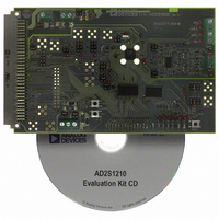
EVAL-AD2S1210EDZ Summary of contents
Page 1
FEATURES Complete monolithic resolver-to-digital converter 3125 rps maximum tracking rate (10-bit resolution) ±2.5 arc minutes of accuracy 10-/12-/14-/16-bit resolution, set by user Parallel and serial 10-bit to 16-bit data ports Absolute position and velocity outputs System fault detection Programmable fault ...
Page 2
AD2S1210 TABLE OF CONTENTS Features .............................................................................................. 1 Applications ....................................................................................... 1 Functional Block Diagram .............................................................. 1 General Description ......................................................................... 1 Product Highlights ........................................................................... 1 Revision History ............................................................................... 2 Specifications ..................................................................................... 3 Timing Specifications .................................................................. 6 Absolute Maximum Ratings ............................................................ 8 ESD ...
Page 3
SPECIFICATIONS = 5.0 V ± 5%, CLKIN = 8.192 MHz ± 25%, EXC, EXC frequency = 10 kHz to 20 kHz (10-bit); 6 kHz to 20 kHz (12-bit kHz to 12 kHz (14-bit); 2 ...
Page 4
AD2S1210 Parameter Tracking Rate 10-bit 12-bit 14-bit 16-bit Acceleration Error 10-bit 12-bit 14-bit 16-bit Settling Time 10° Step Input 10-bit 12-bit 14-bit 16-bit Settling Time 179° Step Input 10-bit 12-bit 14-bit 16-bit EXC, EXC OUTPUTS Voltage Center Voltage Frequency EXC/EXC ...
Page 5
Parameter POWER REQUIREMENTS DRIVE POWER SUPPLY I AVDD I DVDD I OVDD 1 Temperature ranges are as follows grades: –40°C to +85° grades: –40°C to +125°C. 2 The voltages, SIN, SINLO, ...
Page 6
AD2S1210 TIMING SPECIFICATIONS 5.0 V ± 5 MIN Table 2. Parameter Description f Frequency of clock input CLKIN t Clock period ( = 1 and ...
Page 7
Parameter Description t Delay WR/FSYNC rising edge to SDO high Delay from SAMPLE before WR/FSYNC falling edge 30 t Delay CS falling edge to WR/FSYNC falling edge in normal mode and A1 setup time before ...
Page 8
AD2S1210 ABSOLUTE MAXIMUM RATINGS Table 3. Parameter AV to AGND, DGND AGND, DGND AGND, DGND DRIVE AGND to DGND Analog Input Voltage to AGND Digital Input Voltage to DGND ...
Page 9
PIN CONFIGURATION AND FUNCTION DESCRIPTIONS Table 4. Pin Function Descriptions Pin No. Mnemonic Description 1 RES1 Resolution Select 1. Logic input. RES1 in conjunction with RES0 allows the resolution of the AD2S1210 to be programmed. Refer to the Configuration of ...
Page 10
AD2S1210 Pin No. Mnemonic Description 13 DB13/SCLK Data Bit 13/Serial Clock. In parallel mode, this pin acts as DB13, a three-state data output pin controlled by CS and RD. In serial mode, this pin acts as the serial clock input. ...
Page 11
TYPICAL PERFORMANCE CHARACTERISTICS T = 25° SIN/SINLO = 3.15 V p-p, COS/COSLO = 3.15 V p-p, CLKIN = 8.192 MHz , unless otherwise noted DRIVE 9000 8000 7000 6000 ...
Page 12
AD2S1210 12000 10000 8000 6000 4000 2000 0 126 127 128 CODES Figure 9. Typical 10-Bit Angular Accuracy Histogram of Codes, 10,000 Samples, Hysteresis Enabled ...
Page 13
TIME (ms) Figure 15. Typical 14-Bit 179° Step Response 250 225 200 175 150 125 100 ...
Page 14
AD2S1210 5000 10000 15000 20000 25000 30000 35000 40000 45000 2 ACCELERATION (rps ) Figure 21. Typical 14-Bit Tracking Error vs. Acceleration ...
Page 15
RESOLVER FORMAT SIGNALS × sin(ω θ × sin(ωt) × sin(θ (A) CLASSICAL RESOLVER A resolver is a rotating transformer, typically with a primary winding on the ...
Page 16
AD2S1210 THEORY OF OPERATION RESOLVER TO DIGITAL CONVERSION The AD2S1210 operates on a Type II tracking closed-loop principle. The output continually tracks the position of the resolver without the need for external conversion and wait states. As the resolver moves ...
Page 17
Angular Latency = ⎡ LOS threshold × ⎢ 2 Arc cos ⎢ max sine / cosine amplitude ⎣ The preceding equation is based on the worst-case angular error, which can be seen by the AD2S1210 before an LOS fault is ...
Page 18
... The synthetic reference reduces the phase shift between the refer- ence and sine/cosine inputs to less than 10°, and operates for phase shifts of ± ...
Page 19
4.7µF 10nF 10nF 10µ 10nF 4.7µF DGND 5 AD2S1210 CLKIN 7 XTALOUT 8.192 ...
Page 20
AD2S1210 CONFIGURATION OF AD2S1210 MODES OF OPERATION The AD2S1210 has two modes of operation: configuration mode and normal mode. The configuration mode is used to program the registers that set the excitation frequency, the resolution, and the fault detection thresholds ...
Page 21
REGISTER MAP Table 10. Register Map Register Register Register Name Address Data Position 0x80 D15 to D8 0x81 Velocity 0x82 D15 to D8 0x83 LOS Threshold 0x88 DOS Overrange 0x89 D7 ...
Page 22
AD2S1210 DOS RESET MAXIMUM AND MINIMUM THRESHOLD REGISTERS Table 16. 8-Bit Registers Address Bit Read/Write 0x8B Read/write 0x8C Read/write The AD2S1210 continuously stores the minimum and maximum magnitude of the monitor signal in internal ...
Page 23
Address/Data Bit The MSB of each 8-bit word written to the AD2S1210 indicates whether the 8-bit word is a register address or data. The MSB (D7) of each register address defined on the AD2S1210 is high. The MSB of each ...
Page 24
AD2S1210 DIGITAL INTERFACE The angular position and angular velocity are represented by binary data and can be extracted either via a 16-bit parallel interface or via a 4-wire serial interface that operates at clock rates MHz. ...
Page 25
Clearing the Fault Register The LOT pin and/or the DOS pin of the AD2S1210 are taken low to indicate that a fault has been detected. The AD2S1210 is capable of detecting eight separate fault conditions. To determine which condition triggered ...
Page 26
AD2S1210 f CLKIN CLKIN A0 DB0 TO DB7 NOTES 1. DON’T CARE. f CLKIN CLKIN t 16 SAMPLE CS RD A0, A1 DATA *ASSUMES FAULT REGISTER ADDRESS WRITTEN TO PART BEFORE EXITING CONFIGURATION MODE. NOTES 1. ...
Page 27
CLKIN CLKIN t 16 SAMPLE A0, A1 DATA NOTES 1. DON’T CARE. Figure 31. Parallel Port—Clear Fault Register CONFIGURATION 14A t ...
Page 28
AD2S1210 SERIAL INTERFACE The serial interface is selected by holding the SOE pin low. The AD2S1210 serial interface consists of four signals: SDO, SDI FSYNC , and SCLK. The SDI is used for transferring data into the on-chip ...
Page 29
WR/FSYNC t 22 SCLK t 23 MSB SDO MSB SDI Figure 32. Serial Interface Timing Diagram f CLKIN CLKIN WR/FSYNC SDI ADDRESS OLD DATA SDO NOTES 1. DON’T CARE. Figure 33. Serial Interface ...
Page 30
AD2S1210 f CLKIN CLKIN t 16 SAMPLE CS WR/FSYNC A0, A1 SDO *ASSUMES FAULT REGISTER ADDRESS WRITTEN TO PART BEFORE EXITING CONFIGURATION MODE. NOTES 1. DON’T CARE POSITION ...
Page 31
INCREMENTAL ENCODER OUTPUTS The A, B, and NM incremental encoder emulation outputs are free running and are valid if the resolver format input signals applied to the converter are valid. The AD2S1210 can be configured to emulate a 256-line, a ...
Page 32
AD2S1210 CIRCUIT DYNAMICS LOOP RESPONSE MODEL ERROR (ACCELERATION) VELOCITY c 1 – az θ k1 × –1 1 – – bz – Sin/Cos LOOKUP Figure 38. RDC System Response Block Diagram The RDC is a mixed-signal ...
Page 33
Table 29. Loop Transfer Function Parameters vs. Resolution (f = 8.192 MHz) CLKIN Resolution (Bits) t (ms) t (ms 0 160 16 8 728 Note that the closed-loop response is described ...
Page 34
... AD2S1210BSTZ −40°C to +85°C AD2S1210CSTZ −40°C to +125°C AD2S1210DSTZ −40°C to +125°C AD2S1210WDSTZ 2 −40°C to +125°C 2 AD2S1210WDSTZRL7 −40°C to +125°C EVAL-AD2S1210EDZ RoHS Compliant Part. 2 Qualified for Automotive. 9.20 9.00 SQ 0.75 1.60 8.80 0.60 MAX 0.45 ...
Page 35
NOTES Rev Page AD2S1210 ...
Page 36
AD2S1210 NOTES ©2008–2010 Analog Devices, Inc. All rights reserved. Trademarks and registered trademarks are the property of their respective owners. D07467-0-2/10(A) Rev Page ...