MCP1630RD-DDBK3 Microchip Technology, MCP1630RD-DDBK3 Datasheet - Page 10
MCP1630RD-DDBK3
Manufacturer Part Number
MCP1630RD-DDBK3
Description
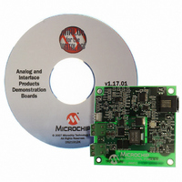
REF DESIGN MCP1630V BI-DIR 4CELL
Manufacturer
Microchip Technology
Type
Battery Managementr
Specifications of MCP1630RD-DDBK3
Main Purpose
Power Management, Battery Charger
Embedded
Yes, MCU, 8-Bit
Utilized Ic / Part
MCP1630
Primary Attributes
4 Cells- Li-Ion, 6.5 ~ 7 V Input
Secondary Attributes
MCU Generates Frequency, 94% Efficiency, 2 Status LEDs
Input Voltage
6.5 V to 7 V
Product
Power Management Modules
For Use With/related Products
MCP1630V, PIC16F88, MCP6022
Lead Free Status / RoHS Status
Not applicable / Not applicable
Lead Free Status / RoHS Status
Lead free / RoHS Compliant, Not applicable / Not applicable


MCP1630/MCP1630V
Note: Unless otherwise noted, V
values = 5.0V, T
FIGURE 2-13:
R
FIGURE 2-14:
Voltage vs. Input Voltage.
FIGURE 2-15:
Voltage vs. Input Voltage.
DS21896B-page 10
DSON
18
16
14
12
10
vs. Input Voltage.
-100
-150
-200
-250
-100
-150
-200
150
100
8
6
4
2
0
-50
-50
50
0
0
A
= -40°C to +125°C.
T
T
A
T
A
= + 25°C
A
= + 25°C
= - 40°C
T
EXT Output P-channel
A
Error Amplifier Input Offset
Error Amplifier Input Offset
T
T
= + 125°C
T
Input Voltage (V)
A
A
Input Voltage (V)
Input Voltage (V)
A
= + 25°C
= + 125°C
= - 40°C
T
A
T
= + 125°C
A
= - 40°C
IN
= 3.0V to 5.5V, F
V
V
CM IN
CM IN
= 1.2V
= 0V
OSC
= 1 MHz with 10% Duty Cycle, C
FIGURE 2-16:
Mode Input Voltage Range vs. Input Voltage
(MCP1630V).
FIGURE 2-17:
Delay vs. Input Voltage (MCP1630V).
2.7
2.4
2.1
1.8
1.5
30
25
20
15
10
3
5
0
3
3.5
T
A
Current Sense Common
Current Sense to V
Input Voltage (V)
Input Voltage (V)
= -40°C
© 2005 Microchip Technology Inc.
4
IN
= 0.1 µF, V
CS Common Mode
Input Range
4.5
T
A
= +125°C
T
A
T
= +25°C
5
A
IN
= +25°C
EXT
for typical
5.5
Related parts for MCP1630RD-DDBK3
Image
Part Number
Description
Manufacturer
Datasheet
Request
R

Part Number:
Description:
REF DESIGN MCP1630 NIMH BATT CHG
Manufacturer:
Microchip Technology
Datasheet:

Part Number:
Description:
BOARD DEMO FOR MCP1630 LI-ION
Manufacturer:
Microchip Technology
Datasheet:

Part Number:
Description:
REFERENCE DESIGN FOR MCP1630
Manufacturer:
Microchip Technology
Datasheet:

Part Number:
Description:
MCP1630 Dual Synchronous Buck Regulator Demo Board DEVTOOL - Analog
Manufacturer:
Microchip Technology
Datasheet:
Part Number:
Description:
Power Management IC Development Tools MCP1630 Sepic Automotive LED Drvr
Manufacturer:
Microchip Technology
Datasheet:

Part Number:
Description:
Manufacturer:
Microchip Technology Inc.
Datasheet:
Part Number:
Description:
Manufacturer:
Microchip Technology Inc.
Datasheet:
Part Number:
Description:
Manufacturer:
Microchip Technology Inc.
Datasheet:
Part Number:
Description:
Manufacturer:
Microchip Technology Inc.
Datasheet:
Part Number:
Description:
Manufacturer:
Microchip Technology Inc.
Datasheet:
Part Number:
Description:
Manufacturer:
Microchip Technology Inc.
Datasheet: