MCP1631RD-MCC2 Microchip Technology, MCP1631RD-MCC2 Datasheet - Page 8
MCP1631RD-MCC2
Manufacturer Part Number
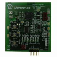
MCP1631RD-MCC2
Description
REFERENCE DESIGN MCP1631HV
Manufacturer
Microchip Technology
Datasheets
1.MCP1631VHVT-330EST.pdf
(34 pages)
2.MCP1631HV-330EST.pdf
(54 pages)
3.MCP1631RD-MCC2.pdf
(20 pages)
4.MCP1631RD-MCC2.pdf
(328 pages)
Specifications of MCP1631RD-MCC2
Main Purpose
Power Management, Battery Charger
Embedded
Yes, MCU, 8-Bit
Utilized Ic / Part
MCP1631HV, PIC16F883
Primary Attributes
1 ~ 2 Cell- Li-Ion, 1 ~ 5 Cell- NiCd/NiMH, 1 ~ 2 1W LEDs
Secondary Attributes
Status LEDs
Silicon Manufacturer
Microchip
Application Sub Type
Battery Charger
Kit Application Type
Power Management - Battery
Silicon Core Number
MCP1631HV, PIC16F883
Kit Contents
Board
Lead Free Status / RoHS Status
Lead free / RoHS Compliant
Lead Free Status / RoHS Status
Lead free / RoHS Compliant


MCP1631/HV/MCP1631V/VHV
DC CHARACTERISTICS (CONTINUED)
TEMPERATURE SPECIFICATIONS
DS22063B-page 8
Electrical Specifications: Unless otherwise noted, V
V
Line Regulation
Load Regulation
Dropout Voltage
Note 2, Note 5
Output Delay Time
Output Noise
Power Supply Ripple Rejection
Ratio
Protection Features
Thermal Shutdown
Thermal Shutdown Hysteresis
Note 1:
Electrical Specifications: Unless otherwise indicated, all limits are specified for: V
Temperature Ranges
Operating Junction Temperature
Range
Storage Temperature Range
Maximum Junction Temperature
Package Thermal Resistances
Thermal Resistance, 20L-TSSOP
Thermal Resistance, 20L-SSOP
Thermal Resistance, 20L-QFN
DD
for typical values = 5.0V, T
2:
3:
4:
5:
Parameters
External Oscillator Input (OSC
characterization testing. Signal levels between 0.8V and 2.0V with rise and fall times measured between 10% and 90%
of maximum and minimum values. Not production tested. Additional timing specifications were fully characterized and
specified that are not production tested.
The minimum V
TCV
temperature range. V
Load regulation is measured at a constant junction temperature using low duty cycle pulse testing. Changes in output
voltage due to heating effects are determined using thermal regulation specification TCV
Dropout voltage is defined as the input to output differential at which the output voltage drops 2% below its measured
value with an applied input voltage of V
Parameters
OUT
= (V
OUT-HIGH
IN
must meet two conditions: V
A
for typical values = +25°C, T
OUT-LOW
- V
V
(V
T
OUT-LOW
DROPOUT
ΔV
ΔV
T
SHD_HYS
PSRR
OUT
V
T
Sym
DELAY
V
e
SHD
OUT
OUT
OUT
IN
N
IN
= lowest voltage measured over the temperature range.
XΔ
)
Sym
θ
θ
θ
) rise and fall times between 10 ns and 10 µs were determined during device
T
T
T
/
/
JA
JA
JA
A
J
J
) *10
6
OUT(MAX)
/ (V
IN
Min
-0.3
-2.5
Min
—
—
—
—
—
—
—
-40
-65
—
—
—
—
= 3.0V to 5.5V, F
R
* ΔTemperature), V
IN
+ V
A
≥ 3.5V and V
= -40°C to +125°C for all minimum and maximums.
DROPOUT(MAX)
89.3
Typ
90
43
—
—
—
1000
±0.1
±1.0
Typ
330
525
150
44
18
8
OSC
IN
+125
+150
+150
≥ (V
OUT-HIGH
Max
= 1 MHz with 10% Duty Cycle, C
—
—
—
Max
+0.3
+2.5
650
725
or 3.5V, whichever is greater.
—
—
—
—
—
OUT(MAX)
IN
+ 3.0V to 5.5V
= highest voltage measured over the
Units
(Hz)
°C/W
°C/W
°C/W
Units
%/V
°C
°C
°C
µV/
mV
mV
dB
µs
°C
°C
%
+ V
1/2
DROPOUT(MAX)
Steady State
Transient
Typical 4 Layer board with
interconnecting vias
Typical 4 Layer board with
interconnecting vias
Typical 4 Layer board with
interconnecting vias
(V
V
I
I
I
V
I
1 µF
f = 100 Hz, C
I
V
C
© 2008 Microchip Technology Inc.
L
L
L
R
L
L
IN
IN
INAC
IN
OUT(MAX)
= 1.0 mA to 250 mA, Note 4
= 250 mA, V
= 250 mA, V
L
= 50 mA, f = 1 kHz, C
= 100 µA,
OUT
= 50Ω resistive
= 0V to 6V, V
= 0 µF, V
≤ 16V Note 2
=100 mV pk-pk,
.
Conditions
Conditions
).
+ V
R
OUT
IN
R
R
= 1.2V
DROPOUT(MAX)
= 0.1 µF,
= 5.0V
= 3.3V
OUT
= 1 µF,
= 90% V
OUT
=
) ≤
R
,
Related parts for MCP1631RD-MCC2
Image
Part Number
Description
Manufacturer
Datasheet
Request
R

Part Number:
Description:
REFERENCE DESIGN FOR MCP1631HV
Manufacturer:
Microchip Technology
Datasheet:

Part Number:
Description:
REF DES BATT CHARG OR LED DRIVER
Manufacturer:
Microchip Technology
Datasheet:

Part Number:
Description:
Manufacturer:
Microchip Technology Inc.
Datasheet:
Part Number:
Description:
Manufacturer:
Microchip Technology Inc.
Datasheet:
Part Number:
Description:
Manufacturer:
Microchip Technology Inc.
Datasheet:
Part Number:
Description:
Manufacturer:
Microchip Technology Inc.
Datasheet:
Part Number:
Description:
Manufacturer:
Microchip Technology Inc.
Datasheet:
Part Number:
Description:
Manufacturer:
Microchip Technology Inc.
Datasheet:
Part Number:
Description:
Manufacturer:
Microchip Technology Inc.
Datasheet:
Part Number:
Description:
Manufacturer:
Microchip Technology Inc.
Datasheet: