UM232R FTDI, Future Technology Devices International Ltd, UM232R Datasheet - Page 6
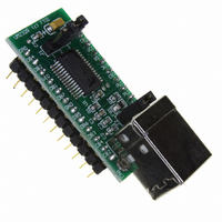
UM232R
Manufacturer Part Number
UM232R
Description
MODULE USB-SER UART FT232 24-DIP
Manufacturer
FTDI, Future Technology Devices International Ltd
Datasheet
1.UM232R.pdf
(28 pages)
Specifications of UM232R
Main Purpose
Interface, USB 2.0 to UART (RS232) Bridge
Embedded
No
Utilized Ic / Part
FT232R
Primary Attributes
Full Speed, Rates of 300 ~ 3 MBaud, Security ID Number
Secondary Attributes
6 ~ 48MHz Clock Generator Output, Royalty-Free Drivers
Lead Free Status / RoHS Status
Lead free / RoHS Compliant
Other names
768-1019


Document Reference No.: FT_000051
UM232R USB - Serial UART Development Module Incorporating Clock Generator
Datasheet Version 1.04
Clearance No.: FTDI# 125
3
FT232RL Features and Enhancement
3.1
Key Features
This section summarises the key features and enhancements of the FT232RL IC device which is used on the
UM232R Module. For further details, consult the FT232R datasheet, which is available from
www.ftdichip.com.
Integrated Clock Circuit - Previous generations of FTDI‟s USB UART devices required an external crystal
or ceramic resonator. The clock circuit has now been integrated onto the device meaning that no crystal or
ceramic resonator is required. However, if preferred, an external 12MHz crystal can be used as the clock
source.
Integrated
EEPROM - Previous generations of FTDI‟s USB UART devices required an external EEPROM if the device
were to use USB Vendor ID (VID), Product ID (PID), serial number and product description strings other
than the default values in the device itself. This external EEPROM has now been integrated onto the FT232R
chip meaning that all designs have the option to change the product description strings. A user area of the
internal EEPROM is available for storing additional data. The internal EEPROM is programmable in circuit,
over USB without any additional voltage requirement.
Preprogrammed EEPROM
- The FT232R is supplied with its internal EEPROM pre-programmed with a serial number which is unique to
each individual device. This, in most cases, will remove the need to program the device EEPROM.
Integrated USB Resistors - Previous generations of FTDI‟s USB UART devices required two external
series resistors on the USBDP and USBDM lines, and a 1.5 kΩ pull up resistor on USBDP. These three
resistors have now been integrated onto the device.
Integrated AVCC Filtering - Previous generations of FTDI‟s USB UART devices had a separate AVCC pin –
the supply to the internal PLL. This pin required an external R-C filter. The separate AVCC pin is now
connected internally to VCC, and the filter has now been integrated onto the chip.
Less External Components - Integration of the crystal, EEPROM, USB resistors, and AVCC filter will
substantially reduce the bill of materials cost for USB interface designs using the FT232R compared to its
FT232BM predecessor.
Configurable CBUS I/O Pin Options - There are now 5 configurable Control Bus (CBUS) lines. Options
are TXDEN - transmit enable for RS485 designs, PWREN# - Power control for high power, bus powered
designs, TXLED# - for pulsing an LED upon transmission of data, RXLED# - for pulsing an LED upon
receiving data, TX&RXLED# - which will pulse an LED upon transmission OR reception of data, SLEEP# -
indicates that the device going into USB suspend mode, CLK48 / CLK24 / CLK12 / CLK6 - 48MHz,
24MHz,12MHz, and 6MHz clock output signal options. There is also the option to bring out bit bang mode
read and write strobes (see below). The CBUS lines can be configured with any one of these output options
by setting bits in the internal EEPROM. The device is supplied with the most commonly used pin definitions
pre-programmed - see
Section 9
for details.
Enhanced Asynchronous Bit Bang Mode with RD# and WR# Strobes - The FT232R supports FTDI‟s
BM chip bit bang mode. In bit bang mode, the eight UART lines can be switched from the regular interface
mode to an 8-bit general purpose I/O port. Data packets can be sent to the device and they will be
sequentially sent to the interface at a rate controlled by an internal timer (equivalent to the baud rate
prescaler). With the FT232R device this mode has been enhanced so that the internal RD# and WR#
strobes are now brought out of the device which can be used to allow external logic to be clocked by
accesses to the bit bang I/O bus. This option will be described more fully in a separate application note.
Synchronous Bit Bang Mode - Synchronous bit bang mode differs from asynchronous bit bang mode in
that the interface pins are only read when the device is written to. Thus making it easier for the controlling
program to measure the response to an output stimulus as the data returned is synchronous to the output
data. The feature was previously seen in FTDI‟s FT2232C device. This option will be described more fully in
a separate application note.
CBUS Bit Bang Mode -
This mode allows four of the CBUS pins to be individually configured as GPIO pins, similar to Asynchronous
bit bang mode. It is possible to use this mode while the UART interface is being used, thus providing up to
four general purpose I/O pins which are available during normal operation. An application note describing
this feature is available separately from www.ftdichip.com.
Lower Supply Voltage - Previous
generations of the chip required 5V supply on the VCC pin. The FT232R will work with a VCC supply in the
range 3.5V to 5.25V. Bus powered designs would still take their supply from the 5V on the USB bus, but for
self powered designs where only 3.5V is available and there is no 5V supply there is no longer any need for
an additional external regulator.
Integrated Level Converter on UART Interface and Control Signals - VCCIO pin supply can be from
1.8V to 5V. Connecting the VCCIO pin to 1.8V, 2.8V, or 3.3V allows the device to directly interface to 1.8V,
© Copyright 2009 Future Technology Devices International Ltd
5
Related parts for UM232R
Image
Part Number
Description
Manufacturer
Datasheet
Request
R

Part Number:
Description:
IC USB TO SERIAL UART 32-QFN
Manufacturer:
FTDI, Future Technology Devices International Ltd

Part Number:
Description:
IC USB HOST CTLR VINCULUM 48LQFP
Manufacturer:
FTDI, Future Technology Devices International Ltd
Datasheet:

Part Number:
Description:
IC USB HOST VINCULUM-II 32QFN
Manufacturer:
FTDI, Future Technology Devices International Ltd
Datasheet:
Part Number:
Description:
IC USB HOST VINCULUM-II 32LQFN
Manufacturer:
FTDI, Future Technology Devices International Ltd
Datasheet:
Part Number:
Description:
IC USB HOST VINCULUM-II 48QFN
Manufacturer:
FTDI, Future Technology Devices International Ltd
Datasheet:
Part Number:
Description:
IC USB HOST VINCULUM-II 32LQFN
Manufacturer:
FTDI, Future Technology Devices International Ltd
Datasheet:
Part Number:
Description:
IC USB HOST VINCULUM-II 32QFN
Manufacturer:
FTDI, Future Technology Devices International Ltd
Datasheet:
Part Number:
Description:
IC USB HOST VINCULUM-II 48LQFP
Manufacturer:
FTDI, Future Technology Devices International Ltd
Datasheet:
Part Number:
Description:
IC USB HOST VINCULUM-II 48LQFP
Manufacturer:
FTDI, Future Technology Devices International Ltd
Datasheet:
Part Number:
Description:
IC USB HOST VINCULUM-II 48QFN
Manufacturer:
FTDI, Future Technology Devices International Ltd
Datasheet:
Part Number:
Description:
IC USB HOST CTLR VINCULUM 64QFN
Manufacturer:
FTDI, Future Technology Devices International Ltd
Datasheet:

Part Number:
Description:
IC USB HOST CTLR VINCULUM 64LQFP
Manufacturer:
FTDI, Future Technology Devices International Ltd
Datasheet:
Part Number:
Description:
IC USB HOST VINCULUM-II 64LQFP
Manufacturer:
FTDI, Future Technology Devices International Ltd
Datasheet:
Part Number:
Description:
IC USB HOST VINCULUM-II 64QFN
Manufacturer:
FTDI, Future Technology Devices International Ltd
Datasheet:

Part Number:
Description:
IC USB TO PARALLEL FIFO 28-SSOP
Manufacturer:
FTDI, Future Technology Devices International Ltd
Datasheet: