C8051T610DB28 Silicon Laboratories Inc, C8051T610DB28 Datasheet - Page 34
C8051T610DB28
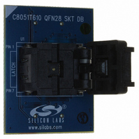
Manufacturer Part Number
C8051T610DB28
Description
DAUGHTER BOARD T610 28QFN SOCKET
Manufacturer
Silicon Laboratories Inc
Datasheet
1.C8051T610DB32.pdf
(218 pages)
Specifications of C8051T610DB28
Module/board Type
Socket Module - QFN
Processor To Be Evaluated
C8051T61x
Interface Type
USB
Lead Free Status / RoHS Status
Lead free / RoHS Compliant
For Use With/related Products
C8051T610DK
Lead Free Status / RoHS Status
Lead free / RoHS Compliant, Lead free / RoHS Compliant
Other names
336-1506


C8051T610/1/2/3/4/5/6/7
Table 7.4. Reset Electrical Characteristics
–40 to +85 °C unless otherwise specified.
Table 7.5. Internal Voltage Regulator Electrical Characteristics
–40 to +85 °C unless otherwise specified.
Table 7.6. EPROM Electrical Characteristics
34
Parameter
Input Voltage Range
Bias Current
Parameter
RST Output Low Voltage
RST Input High Voltage
RST Input Low Voltage
RST Input Pullup Current
V
V
Missing Clock Detector
Timeout
Reset Time Delay
Minimum RST Low Time to
Generate a System Reset
V
V
Parameter
EPROM Size
EPROM Size
Write Cycle Time (per Byte)
Programming Voltage (V
Notes:
DD
DD
DD
DD
1. 512 bytes at location 0x3E00 to 0x3FFF are not available for program storage
2. Refer to device errata for details
POR Ramp Time
Monitor Threshold (V
Monitor Turn-on Time
Monitor Supply Current
PP
RST
)
2
Normal Mode
)
C8051T610/1/6/7
C8051T612/3/4/5
Date Code 0935 and Later
Date Code prior to 0935
I
V
RST = 0.0 V
Time from last system clock
rising edge to reset initiation
Delay between release of any
reset source and code
execution at location 0x0000
V
OL
DD
DD
= 8.5 mA,
= 1.8 V to 3.6 V
= V
Conditions
RST
Conditions
Conditions
- 0.1 V
Rev 1.0
16384
8192
0.75 x V
5.75
6.25
Min
105
Min
500
1.7
15
—
—
—
—
—
—
—
1
Min
1.8
—
DD
6.325
Typ
155
6.0
—
—
1.75
Typ
625
25
50
20
—
—
—
—
—
—
Typ
30
—
Max
6.25
205
6.5
—
—
Max
750
0.6
0.6
1.8
50
60
30
—
—
—
Max
1
3.6
50
Units
bytes
bytes
µs
Units
V
V
Units
V
µA
ms
µA
µA
µs
µs
µs
µs
V
V
V
V
DD
Related parts for C8051T610DB28
Image
Part Number
Description
Manufacturer
Datasheet
Request
R

Part Number:
Description:
SMD/C°/SINGLE-ENDED OUTPUT SILICON OSCILLATOR
Manufacturer:
Silicon Laboratories Inc
Part Number:
Description:
Manufacturer:
Silicon Laboratories Inc
Datasheet:
Part Number:
Description:
N/A N/A/SI4010 AES KEYFOB DEMO WITH LCD RX
Manufacturer:
Silicon Laboratories Inc
Datasheet:
Part Number:
Description:
N/A N/A/SI4010 SIMPLIFIED KEY FOB DEMO WITH LED RX
Manufacturer:
Silicon Laboratories Inc
Datasheet:
Part Number:
Description:
N/A/-40 TO 85 OC/EZLINK MODULE; F930/4432 HIGH BAND (REV E/B1)
Manufacturer:
Silicon Laboratories Inc
Part Number:
Description:
EZLink Module; F930/4432 Low Band (rev e/B1)
Manufacturer:
Silicon Laboratories Inc
Part Number:
Description:
I°/4460 10 DBM RADIO TEST CARD 434 MHZ
Manufacturer:
Silicon Laboratories Inc
Part Number:
Description:
I°/4461 14 DBM RADIO TEST CARD 868 MHZ
Manufacturer:
Silicon Laboratories Inc
Part Number:
Description:
I°/4463 20 DBM RFSWITCH RADIO TEST CARD 460 MHZ
Manufacturer:
Silicon Laboratories Inc
Part Number:
Description:
I°/4463 20 DBM RADIO TEST CARD 868 MHZ
Manufacturer:
Silicon Laboratories Inc
Part Number:
Description:
I°/4463 27 DBM RADIO TEST CARD 868 MHZ
Manufacturer:
Silicon Laboratories Inc
Part Number:
Description:
I°/4463 SKYWORKS 30 DBM RADIO TEST CARD 915 MHZ
Manufacturer:
Silicon Laboratories Inc
Part Number:
Description:
N/A N/A/-40 TO 85 OC/4463 RFMD 30 DBM RADIO TEST CARD 915 MHZ
Manufacturer:
Silicon Laboratories Inc
Part Number:
Description:
I°/4463 20 DBM RADIO TEST CARD 169 MHZ
Manufacturer:
Silicon Laboratories Inc