CY3280-BBM Cypress Semiconductor Corp, CY3280-BBM Datasheet - Page 5
CY3280-BBM
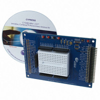
Manufacturer Part Number
CY3280-BBM
Description
MODULE BREADBOARD CAPSENSE
Manufacturer
Cypress Semiconductor Corp
Series
CapSense™r
Datasheet
1.CY3280-BBM.pdf
(8 pages)
Specifications of CY3280-BBM
Mfg Application Notes
Capacitance Sensing - AppNote CapSense Best Practices - AppNote
Design Resources
CY3280-BBM Schematic
Accessory Type
Prototyping Board
Interface Type
Serial
Operating Voltage
5 V
Silicon Manufacturer
Cypress
Silicon Core Number
CAP1073264
Kit Application Type
Sensing - Touch / Proximity
Application Sub Type
Capacitive Touch
Rohs Compliant
No
Lead Free Status / RoHS Status
Lead free / RoHS Compliant
For Use With/related Products
CY3280 Module Board
For Use With
428-2987 - CAPSENSE CONTROLLER DEV KIT
Lead Free Status / Rohs Status
Lead free / RoHS Compliant
Other names
428-2992


GND spacing is
generalized for
noise immunity
and sensitivity.
Connection to
shield
electrode is
through a
jumper.
ESD protection
circuitry is not
included.
User Module
Parameters set
to supplied
overlay
thicknesses.
Unused pins
are not routed
directly to
GND.
0-Ω Resistors
populated
throughout.
Feature
Design
Universality of kit
required middle-ground
on many parameters.
Flexibility of module
boards for both CSD and
CSA control boards.
Development/evaluation
platform without
consistent overlay is
inherently vulnerable to
ESD events.
Projects optimized for
supplied hardware.
Pins brought out to
connector for
subsequent modules or
custom designs.
Universality of the board
enabled by population/
depopulation of 0-Ω
resistors.
Reason
Design is not optimized
for high-noise or very
thick overlays.
Higher resistance paths
can impair performance
of shield electrode in
CSD projects.
Direct or air-separated
ESD testing may impair
operation or damage
circuitry. +/-2kV limit on
PSoC pins (see
datasheet).
Sensitivity may not be
high enough for very
thick overlays.
Possible noise path.
Solder pads of 0-Ω
resistors increase
parasitic capacitance.
Impact
Increase spacing for
thicker overlays and
better sensitivity.
Decrease spacing for
greater noise immunity.
Dedicated trace for
shield electrode.
Remove jumpers
wherever possible.
Include an overlay and
ESD protection circuitry.
Thicker overlays may
require verification of
parameters to ensure
proper operation.
Tie unused sensing
traces directly to
ground.
Route traces directly to
sensing elements. Use
as few 0-Ω resistors as
possible.
Recommended
Change
Page: 5
Related parts for CY3280-BBM
Image
Part Number
Description
Manufacturer
Datasheet
Request
R

Part Number:
Description:
KIT UNIVERSAL CAPSENSE CTRLR
Manufacturer:
Cypress Semiconductor Corp
Datasheet:

Part Number:
Description:
BOARD EVAL CAPSENSE EXPRESS
Manufacturer:
Cypress Semiconductor Corp
Datasheet:

Part Number:
Description:
CAPSENSE CONTROLLER DEV KIT
Manufacturer:
Cypress Semiconductor Corp
Datasheet:

Part Number:
Description:
MODULE LINEAR SLIDER CAPSENSE
Manufacturer:
Cypress Semiconductor Corp
Datasheet:

Part Number:
Description:
MODULE RADIAL SLIDER CAPSENSE
Manufacturer:
Cypress Semiconductor Corp
Datasheet:

Part Number:
Description:
MODULE SIMPLE BUTTON CAPSENSE
Manufacturer:
Cypress Semiconductor Corp
Datasheet:

Part Number:
Description:
MODULE MATRIXED BUTTON CAPSENSE
Manufacturer:
Cypress Semiconductor Corp
Datasheet:

Part Number:
Description:
BOARD DEV CAPSENSE CTLR
Manufacturer:
Cypress Semiconductor Corp
Part Number:
Description:
BOARD DEV CAPSENSE CTLR
Manufacturer:
Cypress Semiconductor Corp
Part Number:
Description:
KIT DEV CAPSENSE CTLR UNIV
Manufacturer:
Cypress Semiconductor Corp
Datasheet:

Part Number:
Description:
MODULE CAPSENSE PLUS
Manufacturer:
Cypress Semiconductor Corp
Datasheet:
Part Number:
Description:
SmartSense Evaluation Kit
Manufacturer:
Cypress Semiconductor Corp
Part Number:
Description:
Manufacturer:
Cypress Semiconductor Corp
Datasheet: