PL-BYTEBLASTER2N Altera, PL-BYTEBLASTER2N Datasheet - Page 19
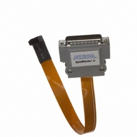
PL-BYTEBLASTER2N
Manufacturer Part Number
PL-BYTEBLASTER2N
Description
CABLE PROGRAMMING PARALLEL PORT
Manufacturer
Altera
Series
ByteBlaster™r
Datasheet
1.PL-BYTEBLASTER2N.pdf
(26 pages)
Specifications of PL-BYTEBLASTER2N
Accessory Type
Download Cable
Core Architecture
FPGA
Core Sub-architecture
Arria, Cyclone, Stratix
Ic Product Type
Debugger / Programmer
Kit Contents
Device, Cable, Guides
Rohs Compliant
Yes
For Use With/related Products
EPCS Serial Configuration Devices
Lead Free Status / RoHS Status
Lead free / RoHS Compliant
Other names
544-1289
PL-BYTEBLASTER2
PL-BYTEBLASTER2
Available stocks
Company
Part Number
Manufacturer
Quantity
Price


Chapter 2: ByteBlaster II Specifications
ByteBlaster II Connections
Table 2–2. ByteBlaster II 25-Pin Header Pin-Outs
ByteBlaster II 10-Pin Header Connection
Table 2–3. ByteBlaster II Female Plug Signal Names and Programming Modes
© July 2008 Altera Corporation
Pin
18 to 25
1
2
3
4
5
6
7
8
11
13
15
5
8
DCLK
GND
CONF_DONE
VCC(TRGT)
nCONFIG
nCE
DATAOUT
nCS
Signal Name
nCE
ASDI
CONF_DONE
DATAOUT
nVCC
Detect
GND
AS Mode
Clock signal
Signal ground
Configuration done
Target power supply
Configuration control nCONFIG
Cyclone chip enable
Active serial data out
Serial configuration
device chip select
The 10-pin female plug connects to a 10-pin male header on the circuit board.
Figure 2–2
Figure 2–2. ByteBlaster II 10-Pin Female Plug Dimensions
Table 2–3
programming mode.
Description
Cyclone chip enable
Active serial data in
Configuration done
Active serial data out
Signal ground
identifies the 10-pin female plug signal names and the corresponding
shows the dimensions of the female plug.
—
0.250 Typ.
Dimensions are shown in inches. Spacing between pin centers is 0.1 inches.
DCLK
GND
CONF_DONE
VCC(TRGT)
nSTATUS
Signal Name
0.425 Typ.
DATA0
CONF_DONE
nSTATUS
nVCC
Detect
GND
—
—
(Part 2 of 2)
10
9
—
8
7
PS Mode
0.100 Sq.
Clock signal
Signal ground
Configuration done
Target power supply
Configuration control TMS
No connect
Configuration status
No connect
0.700 Typ.
5
6
Description
No connect
Data to device
Configuration
done
Signal status
Signal ground
3
4
—
0.025 Sq.
1
2
(Part 1 of 2)
TDI
TDO
nVCC
Detect
GND
TCK
GND
TDO
VCC(TRGT)
Signal Name
ByteBlaster II Download Cable User Guide
—
—
—
—
—
JTAG Mode
Clock signal
Signal ground
Data from device
Target power
supply
JTAG state
machine control
No connect
No connect
No connect
No connect
No connect
Data to device
Data from device
Signal ground
Description
—
2–3
Related parts for PL-BYTEBLASTER2N
Image
Part Number
Description
Manufacturer
Datasheet
Request
R

Part Number:
Description:
CYCLONE II STARTER KIT EP2C20N
Manufacturer:
Altera
Datasheet:


Part Number:
Description:
CPLD, EP610 Family, ECMOS Process, 300 Gates, 16 Macro Cells, 16 Reg., 16 User I/Os, 5V Supply, 35 Speed Grade, 24DIP
Manufacturer:
Altera Corporation
Datasheet:
Part Number:
Description:
CPLD, EP610 Family, ECMOS Process, 300 Gates, 16 Macro Cells, 16 Reg., 16 User I/Os, 5V Supply, 15 Speed Grade, 24DIP
Manufacturer:
Altera Corporation
Datasheet:
Part Number:
Description:
Manufacturer:
Altera Corporation
Datasheet:
Part Number:
Description:
CPLD, EP610 Family, ECMOS Process, 300 Gates, 16 Macro Cells, 16 Reg., 16 User I/Os, 5V Supply, 30 Speed Grade, 24DIP
Manufacturer:
Altera Corporation
Datasheet:
Part Number:
Description:
High-performance, low-power erasable programmable logic devices with 8 macrocells, 10ns
Manufacturer:
Altera Corporation
Datasheet:
Part Number:
Description:
High-performance, low-power erasable programmable logic devices with 8 macrocells, 7ns
Manufacturer:
Altera Corporation
Datasheet:
Part Number:
Description:
Classic EPLD
Manufacturer:
Altera Corporation
Datasheet:
Part Number:
Description:
High-performance, low-power erasable programmable logic devices with 8 macrocells, 10ns
Manufacturer:
Altera Corporation
Datasheet:
Part Number:
Description:
Manufacturer:
Altera Corporation
Datasheet:
Part Number:
Description:
Manufacturer:
Altera Corporation
Datasheet:
Part Number:
Description:
Manufacturer:
Altera Corporation
Datasheet:
Part Number:
Description:
CPLD, EP610 Family, ECMOS Process, 300 Gates, 16 Macro Cells, 16 Reg., 16 User I/Os, 5V Supply, 25 Speed Grade, 24DIP
Manufacturer:
Altera Corporation
Datasheet: