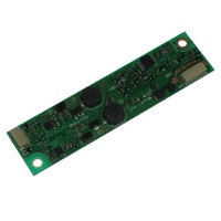
ALD-214012PJ111 TDK Corporation, ALD-214012PJ111 Datasheet

ALD-214012PJ111
Specifications of ALD-214012PJ111
Available stocks
Related parts for ALD-214012PJ111
ALD-214012PJ111 Summary of contents
Page 1
MESSRS : CUSTOMER'S PRODUCT NAME: TDK PRODUCT NAME: PREPARED BY K.Oshima Feb./23th/2010 APPROVED BY AUTHORIZED BY K.Yamaishi H.Masuoka Feb./23th/2010 Feb./23th/2010 DWG.No. D ...
Page 2
D ...
Page 3
This product is conformity to RoHS directive.(*) (*)Conformity to RoHS Directive: This means that, in conformity with EU Directive 2002/95/EC, lead,cadmium,hexavalent chromium, and specific bromine-based flame retardants, PBB and PBDE, have not been used, except for exempted applications. . . ...
Page 4
Outline any parts and pattering inhibit area except GND pattern. TOP View (ii) 8 SIDE View BOTTOM View When LED driver is fixing, please confirm screw head and plate form is located within above hatching area include any tolerances. ...
Page 5
D ...
Page 6
Dec 12.8(at Vin=10.8V) ~44 Minimum load Voltage > Vin+2V Please use it with heat radiated on the worst condition (input voltage, load voltage, mounting instruction, and temperature) when the following standards are used and, that the Q7 transistor package ...
Page 7
Item Symbol Ta(degC) 25±10 Input Current1 Iin1 -30~85 Input Current2 Iin2 25±10 25±10 Iout1-1, Output Current1 Iout2-1, -30~85 Output Current2 Iout1-2, 25±10 (PWM Dimming) Iout2-2 Output Current3 Iout1-3, 25±10 (Analog Dimming) Iout2-3 PWM Burst F 25±10 Frequency Vst1 25±10 Alarm ...
Page 8
Notice of the alarm output The alarm output might be generated at the transition state of ON/OFF by Vrmt or Vin. *4-6 Internal circuit connection It is not a guaranteed ...
Page 9
Others 6-1. Test Conditions Unless otherwise specified test environment is determined as temperature is (20±15)degC and humidity is (65±20)%RH. 6-2. Warranty One year after shippment. Defective products are exchanged during the warranted term free of charge. 6-3. Others ...


