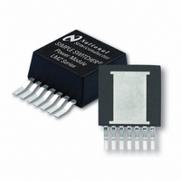
LMZ12001TZE-ADJ/NOPB National Semiconductor, LMZ12001TZE-ADJ/NOPB Datasheet - Page 13

LMZ12001TZE-ADJ/NOPB
Manufacturer Part Number
LMZ12001TZE-ADJ/NOPB
Description
IC BUCK SYNC ADJ 1A TO-PMOD-7
Manufacturer
National Semiconductor
Series
SIMPLE SWITCHER®r
Type
Point of Load (POL) Non-Isolated with UVLOr
Datasheet
1.LMZ12001TZX-ADJNOPB.pdf
(18 pages)
Specifications of LMZ12001TZE-ADJ/NOPB
Output
0.8 ~ 6 V
Number Of Outputs
1
Power (watts)
6W
Mounting Type
Surface Mount
Voltage - Input
4.5 ~ 20V
Package / Case
TO-PMOD-7, Power Module
1st Output
0.8 ~ 6 VDC @ 1A
Size / Dimension
0.40" L x 0.54" W x 0.18" H (10.16mm x 13.77mm x 4.57mm)
Power (watts) - Rated
6W
Operating Temperature
-40°C ~ 125°C
Efficiency
92%
Approvals
EN
Lead Free Status / RoHS Status
Lead free / RoHS Compliant
3rd Output
-
2nd Output
-
Available stocks
Company
Part Number
Manufacturer
Quantity
Price
Following is a comparison pair of waveforms of the showing
both CCM (upper) and DCM operating modes.
The approximate formula for determining the DCM/CCM
boundary is as follows:
I
Following is a typical waveform showing the boundary condi-
tion.
The inductor internal to the module is 10 μH. This value was
chosen as a good balance between low and high input voltage
applications. The main parameter affected by the inductor is
the amplitude of the inductor ripple current (I
calculated with:
I
Where V
mined from equation 10.
If the output current I
I
aware that the lower peak of I
eration is required.
POWER DISSIPATION AND BOARD THERMAL
REQUIREMENTS
For the design case of V
(MAX)
thermal resistance from case to ambient of:
θ
DCB
LR P-P
L
CA
, the higher and lower peak of I
< (T
≊
= 85°C , and T
V
=V
O
J-MAX
*(V
O
IN
*(V
IN
is the maximum input voltage and f
V
CCM and DCM Operating Modes
–V
IN
— T
IN
V
- V
IN
Transition Mode Operation
= 12V, V
O
)/(2*10 μH*f
AMB(MAX)
= 12V, V
O
)/(10µH*f
JUNCTION
O
is determined by assuming that I
O
IN
) / P
O
= 3.3V, I
= 12V, V
SW
= 3.3V, I
= 125°C, the device must see a
SW(CCM)
LR
IC-LOSS
*V
must be positive if CCM op-
IN
LR
) (17)
O
*V
O
O
= 1A/0.25A
can be determined. Be
- θ
= 1.8V, I
= 0.29A
IN
JC
) (16)
(18)
30114814
30114812
LR
O
). I
SW
= 1A, T
LR
is deter-
can be
AMB
O
=
13
Given the typical thermal resistance from junction to case to
be 1.9 °C/W .Use the 85°C power dissipation curves in the
Typical Performance Characteristics section to estimate the
P
it is 0.4W
θ
To reach θ
effectively. With no airflow and no external heat, a good esti-
mate of the required board area covered by 1 oz. copper on
both the top and bottom metal layers is:
Board Area_cm
As a result, approximately 5 square cm of 1 oz copper on top
and bottom layers is required for the PCB design. The PCB
copper heat sink must be connected to the exposed pad. Ap-
proximately thirty six, 10 mils (254 μm) thermal vias spaced
59 mils (1.5 mm) apart must connect the top copper to the
bottom copper. For an example of a high thermal performance
PCB layout, refer to the Evaluation Board application note
AN–2024. For more information on thermal design see AN–
2020 and AN–2026.
PC BOARD LAYOUT GUIDELINES
PC board layout is an important part of DC-DC converter de-
sign. Poor board layout can disrupt the performance of a DC-
DC converter and surrounding circuitry by contributing to EMI,
ground bounce and resistive voltage drop in the traces. These
can send erroneous signals to the DC-DC converter resulting
in poor regulation or instability. Good layout can be imple-
mented by following a few simple design rules.
1. Minimize area of switched current loops.
From an EMI reduction standpoint, it is imperative to minimize
the high di/dt current paths during PC board layout. The high
current loops that do not overlap have high di/dt content that
will cause observable high frequency noise on the output pin
if the input capacitor C
LMZ12001. Therefore physically place C
sible to the LMZ12001 VIN and GND exposed pad. This will
minimize the high di/dt area and reduce radiated EMI. Addi-
tionally, grounding for both the input and output capacitor
should consist of a localized top side plane that connects to
the GND exposed pad (EP).
2. Have a single point ground.
The ground connections for the feedback, soft-start, and en-
able components should be routed to the GND pin of the
device. This prevents any switched or load currents from
flowing in the analog ground traces. If not properly handled,
poor grounding can result in degraded load regulation or er-
ratic output voltage ripple behavior. Provide the single point
ground connection from pin 4 to EP.
CA
IC-LOSS
< (125 — 85) / 0.4W —1.9 = 98.1
for the application being designed. In this application
CA
= 98.1, the PCB is required to dissipate heat
2
= 500°C x cm
IN1
is placed a distance away for the
2
/W / θ
JC
IN1
(19)
asa close as pos-
www.national.com
30114811


