LTM8033EV#PBF Linear Technology, LTM8033EV#PBF Datasheet - Page 8
LTM8033EV#PBF
Manufacturer Part Number
LTM8033EV#PBF
Description
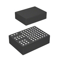
IC DC-DC UMODULE BUCK 3A 76-LGA
Manufacturer
Linear Technology
Series
µModuler
Type
Point of Load (POL) Non-Isolatedr
Datasheet
1.LTM8033MPVPBF.pdf
(24 pages)
Specifications of LTM8033EV#PBF
Output
0.8 ~ 24 V
Number Of Outputs
1
Power (watts)
72W
Mounting Type
Surface Mount
Voltage - Input
3.6 ~ 36 V
Package / Case
76-LGA
1st Output
0.8 ~ 24 VDC @ 3A
Size / Dimension
0.59" L x 0.44" W x 0.17" H (15mm x 11.25mm x 4.32mm)
Power (watts) - Rated
72W
Operating Temperature
-40°C ~ 125°C
Approvals
EN
Lead Free Status / RoHS Status
Lead free / RoHS Compliant
3rd Output
-
2nd Output
-
Available stocks
Company
Part Number
Manufacturer
Quantity
Price


PIN FUNCTIONS
LTM8033
V
capacitor and the output load between these pins and
GND pins.
GND (A8, Bank 2): Tie these GND pins to a local ground
plane below the LTM8033 and the circuit components.
Return the feedback divider (R
FIN (Bank 3): Filtered Input. This is the node after the input
EMI filter. Apply the capacitor recommended by Table 1.
Additional capacitance may be applied if there is a need
to modify the behavior of the integrated EMI filter; other-
wise, leave these pins unconnected. See the Applications
Information section for more details.
V
internal regulator and to the internal power switch. This
pin must be locally bypassed with an external, low ESR
capacitor; see Table 1 for recommended values. Ensure
that V
SHARE (Pin A6): Tie this to the SHARE pin of another
LTM8033 when paralleling the outputs. Otherwise, do
not connect.
ADJ (Pin A7): The LTM8033 regulates its ADJ pin to 0.79V.
Connect the adjust resistor from this pin to ground. The
value of R
– 0.79), where R
RT (Pin B6): The RT pin is used to program the switching
frequency of the LTM8033 by connecting a resistor from
this pin to ground. The Applications Information section of
the data sheet includes a table to determine the resistance
value based on the desired switching frequency. Minimize
8
OUT
IN
(Bank 4): The V
(Bank 1): Power Output Pins. Apply the output filter
IN
+ BIAS is less than 56V.
ADJ
is given by the equation R
ADJ
IN
pin supplies current to the LTM8033’s
is in kΩ.
ADJ
) to this net.
ADJ
= 394.21/(V
OUT
capacitance at this pin.
SYNC (Pin B8): This is the external clock synchronization
input. Ground this pin for low ripple Burst Mode
at low output loads. Tie to a stable voltage source greater
than 0.7V to disable Burst Mode operation. Do not leave
this pin floating. Tie to a clock source for synchronization.
Clock edges should have rise and fall times faster than
1μs. See the Synchronization section in the Applications
Information section.
PGOOD (Pin B7): The PGOOD pin is the open-collector
output of an internal comparator. PGOOD remains low
until the ADJ pin is greater than 90% of the final regulation
voltage. PGOOD output is valid when V
and RUN/SS is high. If this function is not used, leave
this pin floating.
AUX (Pin G3): Low Current Voltage Source for BIAS.
In many designs, the BIAS pin is simply connected to
V
is placed adjacent to the BIAS pin to ease printed circuit
board routing. Although this pin is internally connected
to V
not connect this pin to the load. If this pin is not tied to
BIAS, leave it floating.
BIAS (Pin G4): The BIAS pin connects to the internal power
bus. Connect to a power source greater than 2.8V and less
than 25V. If the output is greater than 2.8V, connect this
pin there. If the output voltage is less, connect this to a
voltage source between 2.8V and 25V but ensure that V
+ BIAS is less than 56V.
RUN/SS (Pin G8): Pull the RUN/SS pin below 0.2V to
shut down the LTM8033. Tie to 2.5V or more for normal
operation. If the shutdown feature is not used, tie this pin
to the V
see the Applications Information section.
OUT
OUT
. The AUX pin is internally connected to V
, it is not intended to deliver a high current, so do
IN
pin. RUN/SS also provides a soft-start function;
IN
is above 3.6V
®
operation
OUT
and
8033f
IN
Related parts for LTM8033EV#PBF
Image
Part Number
Description
Manufacturer
Datasheet
Request
R

Part Number:
Description:
Ultralow Noise Emc 36vin, 3a Dc/dc
Manufacturer:
Linear Technology Corporation
Datasheet:

Part Number:
Description:
BOARD EVAL LTM8003
Manufacturer:
Linear Technology
Datasheet:
Part Number:
Description:
CD ROM LINEARVIEW DATASHEETS
Manufacturer:
Linear Technology
Part Number:
Description:
Standalone Linear Li-Ion Battery Charger with Thermal Regulation in ThinSOT
Manufacturer:
Linear Technology Corporation
Datasheet:
Part Number:
Description:
Low noise, high frequency, 8th order linear phase lowpass filter
Manufacturer:
Linear Technology Corporation
Datasheet:
Part Number:
Description:
Manufacturer:
Linear Technology Corporation
Datasheet:
Part Number:
Description:
Manufacturer:
Linear Technology Corporation
Datasheet:
Part Number:
Description:
Manufacturer:
Linear Technology Corporation
Datasheet:
Part Number:
Description:
Manufacturer:
Linear Technology Corporation
Datasheet:
Part Number:
Description:
Manufacturer:
Linear Technology Corporation
Datasheet:
Part Number:
Description:
Manufacturer:
Linear Technology Corporation
Datasheet:
Part Number:
Description:
Manufacturer:
Linear Technology Corporation
Datasheet:
Part Number:
Description:
Dual and Quad, JFET Input Precision High Speed Op Amps
Manufacturer:
Linear Technology Corporation
Datasheet:
Part Number:
Description:
Manufacturer:
Linear Technology Corporation
Datasheet:
Part Number:
Description:
1, 2, 6 and 8 Channel, 10-Bit Serial I/O Data Acquisition Systems
Manufacturer:
Linear Technology Corporation
Datasheet: