LTM4604IV#PBF Linear Technology, LTM4604IV#PBF Datasheet - Page 6
LTM4604IV#PBF
Manufacturer Part Number
LTM4604IV#PBF
Description
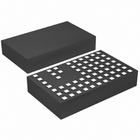
IC DC/DC UMODULE 4A 66-LGA
Manufacturer
Linear Technology
Series
µModuler
Type
Point of Load (POL) Non-Isolatedr
Datasheet
1.LTM4604EVPBF.pdf
(20 pages)
Specifications of LTM4604IV#PBF
Design Resources
LTM4604 Spice Model
Output
0.8 ~ 5 V
Number Of Outputs
1
Power (watts)
20W
Mounting Type
Surface Mount
Voltage - Input
2.38 ~ 5.5 V
Package / Case
66-LGA
1st Output
0.8 ~ 5 VDC @ 4A
Size / Dimension
0.59" L x 0.35" W x 0.09" H (15mm x 9mm x 2.3mm)
Power (watts) - Rated
20W
Operating Temperature
-40°C ~ 85°C
Lead Free Status / RoHS Status
Lead free / RoHS Compliant
3rd Output
-
2nd Output
-
Available stocks
Company
Part Number
Manufacturer
Quantity
Price


PIN FUNCTIONS
LTM4604
V
Apply input voltage between these pins and GND pins.
Recommend placing input decoupling capacitance directly
between V
V
Pins. Apply output load between these pins and GND pins.
Recommend placing output decoupling capacitance directly
between these pins and GND pins. Review Table 4.
GND (G3-G5, F3-F5, E4-E5, A1-A11, B6-B11, C8-C11):
Power Ground Pins for Both Input and Output Returns.
TRACK (E1): Output Voltage Tracking Pin. When the module
is confi gured as a master output, then a soft-start capaci-
tor is placed on the RUN/SS pin to ground to control the
master ramp rate. Slave operation is performed by putting
a resistor divider from the master output to ground, and
connecting the center point of the divider to this pin on
the slave regulator. If tracking is not desired, then connect
the TRACK pin to V
tracking. See Applications Information section.
FB (G2): The Negative Input of the Error Amplifi er. Inter-
nally, this pin is connected to V
6
IN
OUT
(B1, C1, C3-C7, D7, E6 and E7): Power Input Pins.
(D8-D11, E8-E11, F6-F11, G6-G11): Power Output
IN
pins and GND pins.
IN
. Load current must be present for
OUT
with a 4.99k precision
10
11
1
2
3
4
5
6
7
8
9
A
GND
SW
B
V
IN
C
TOP VIEW
TRACK
RUN/
D
SS
GND
resistor. Different output voltages can be programmed
with an additional resistor between FB and GND pins.
Two power modules can current share when this pin is
connected in parallel with the adjacent module’s FB pin.
See Applications Information section.
COMP (G1): Current Control Threshold and Error Amplifi er
Compensation Point. The current comparator threshold
increases with this control voltage. Two power modules
can current share when this pin is connected in parallel
with the adjacent module’s COMP pin.
PGOOD (F1): Output Voltage Power Good Indicator. Open-
drain logic output that is pulled to ground when the output
voltage is not within ±7.5% of the regulation point.
RUN/SS (D1): Run Control and Soft-Start Pin. A voltage
above 0.8V will turn on the module, and below 0.5V will
turn off the module. This pin has a 1M resistor to V
a 1000pF capacitor to GND. See Application Information
section for soft-start information.
SW (B3 and B4): Switching Node of the circuit is used for
testing purposes. This can be connected to copper on the
board to improve thermal performance. Make sure not to
connect it to other output pins.
E
V
OUT
F
PGOOD
G
COMP
FB
IN
4604fa
and
Related parts for LTM4604IV#PBF
Image
Part Number
Description
Manufacturer
Datasheet
Request
R

Part Number:
Description:
Low Voltage, 4A DC/DC ?ModuleTM with Tracking
Manufacturer:
LINER [Linear Technology]
Datasheet:

Part Number:
Description:
IC DC/DC UMODULE 4A 66-LGA
Manufacturer:
Linear Technology
Datasheet:

Part Number:
Description:
CD ROM LINEARVIEW DATASHEETS
Manufacturer:
Linear Technology

Part Number:
Description:
Standalone Linear Li-Ion Battery Charger with Thermal Regulation in ThinSOT
Manufacturer:
Linear Technology Corporation
Datasheet:
Part Number:
Description:
Low noise, high frequency, 8th order linear phase lowpass filter
Manufacturer:
Linear Technology Corporation
Datasheet:
Part Number:
Description:
Manufacturer:
Linear Technology Corporation
Datasheet:
Part Number:
Description:
Manufacturer:
Linear Technology Corporation
Datasheet:
Part Number:
Description:
Manufacturer:
Linear Technology Corporation
Datasheet:
Part Number:
Description:
Manufacturer:
Linear Technology Corporation
Datasheet:
Part Number:
Description:
Manufacturer:
Linear Technology Corporation
Datasheet:
Part Number:
Description:
Manufacturer:
Linear Technology Corporation
Datasheet:
Part Number:
Description:
Manufacturer:
Linear Technology Corporation
Datasheet:
Part Number:
Description:
Dual and Quad, JFET Input Precision High Speed Op Amps
Manufacturer:
Linear Technology Corporation
Datasheet:
Part Number:
Description:
Manufacturer:
Linear Technology Corporation
Datasheet:
Part Number:
Description:
1, 2, 6 and 8 Channel, 10-Bit Serial I/O Data Acquisition Systems
Manufacturer:
Linear Technology Corporation
Datasheet: