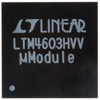
LTM4603HVIV#PBF Linear Technology, LTM4603HVIV#PBF Datasheet - Page 14

LTM4603HVIV#PBF
Manufacturer Part Number
LTM4603HVIV#PBF
Description
IC DC/DC UMODULE 6A 118-LGA
Manufacturer
Linear Technology
Series
µModuler
Type
Point of Load (POL) Non-Isolatedr
Datasheet
1.LTM4603HVEVPBF.pdf
(24 pages)
Specifications of LTM4603HVIV#PBF
Design Resources
LTM4603HV Spice Model
Output
0.6 ~ 5 V
Number Of Outputs
1
Power (watts)
30W
Mounting Type
Surface Mount
Voltage - Input
4.5 ~ 28 V
Package / Case
118-LGA
1st Output
0.6 ~ 5 VDC @ 6A
Size / Dimension
0.59" L x 0.59" W x 0.11" H (15mm x 15mm x 2.8mm)
Power (watts) - Rated
30W
Operating Temperature
-40°C ~ 85°C
Efficiency
93%
Lead Free Status / RoHS Status
Lead free / RoHS Compliant
3rd Output
-
2nd Output
-
Available stocks
Company
Part Number
Manufacturer
Quantity
Price
APPLICATIO S I FOR ATIO
LTM4603HV
to the rising edge of the external clock. The frequency
range is ±30% around the operating frequency of 1MHz.
A pulse detection circuit is used to detect a clock on the
PLLIN pin to turn on the phase lock loop. The pulse width
of the clock has to be at least 400ns and 2V in amplitude.
During the start-up of the regulator, the phase-lock loop
function is disabled.
INTV
An internal low dropout regulator produces an internal
5V supply that powers the control circuitry and DRV
for driving the internal power MOSFETs. Therefore, if the
system does not have a 5V power rail, the LTM4603HV
can be directly powered by Vin. The gate driver current
through the LDO is about 20mA. The internal LDO power
dissipation can be calculated as:
The LTM4603HV also provides the external gate driver
voltage pin DRV
recommended to connect DRV
rail. This is especially true for higher input voltages. Do
not apply more than 6V to the DRV
be used to power the DRV
as shown in Figure 18.
Parallel Operation of the Module
The LTM4603HV device is an inherently current mode
controlled device. Parallel modules will have very good
14
P
LDO_LOSS
2.5
2.0
1.5
1.0
0.5
CC
0
0
and DRV
Figure 7. 1.5V Power Loss
1
= 20mA • (V
OUTPUT CURRENT (A)
2
CC
CC
. If there is a 5V rail in the system, it is
U
3
Connection
12V LOSS
4
U
IN
CC
5
– 5V)
pin with an external circuit
5V LOSS
CC
4603HV F07
6
CC
pin to the external 5V
W
7
pin. A 5V output can
3.5
3.0
2.0
1.5
1.0
2.5
0.5
0
0
U
1
Figure 8. 3.3V Power Loss
CC
OUTPUT CURRENT (A)
2
24V LOSS
3
12V LOSS
current sharing. This will balance the thermals on the
design. The voltage feedback equation changes with the
variable n as modules are paralleled:
n is the number of paralleled modules.
Thermal Considerations and Output Current Derating
The power loss curves in Figures 7 and 8 can be used
in coordination with the load current derating curves in
Figures 9 to 12, and Figures 13 to 16 for calculating an
approximate θ
methods. Thermal models are derived from several tem-
perature measurements at the bench and thermal modeling
analysis. Thermal Application Note 103 provides a detailed
explanation of the analysis for the thermal models and the
derating curves. Tables 3 and 4 provide a summary of the
equivalent θ
θ
and are improved with air fl ow. The case temperature is
maintained at 100°C or below for the derating curves.
This allows for 4W maximum power dissipation in the
total module with top and bottom heatsinking, and 2W
power dissipation through the top of the module with an
approximate θ
to a total of 124°C at the junction of the device.
JA
4
V
parameters are correlated to the measured values,
OUT
5
=
0 6
4603HV F08
6
.
JA
V
JA
JC
for the noted conditions. These equivalent
7
60 4
for the module with various heat sinking
between 6°C/W to 9°C/W. This equates
n
.
R
k
SET
+
6
5
4
3
2
1
0
R
75
SET
5V
5V
5V
AMBIENT TEMPERATURE (°C)
Figure 9. No Heat Sink
IN
IN
IN
80
, 1.5V
, 1.5V
, 1.5V
OUT
OUT
OUT
, 0LFM
, 200LFM
, 400LFM
85
90
4603HV F09
4603hvf
95


