LMZ14201TZ-ADJ/NOPB National Semiconductor, LMZ14201TZ-ADJ/NOPB Datasheet - Page 11
LMZ14201TZ-ADJ/NOPB
Manufacturer Part Number
LMZ14201TZ-ADJ/NOPB
Description
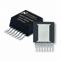
IC BUCK SYNC ADJ 1A TO-PMOD-7
Manufacturer
National Semiconductor
Series
SIMPLE SWITCHER®r
Type
Point of Load (POL) Non-Isolated with UVLOr
Datasheet
1.LMZ14201TZX-ADJNOPB.pdf
(18 pages)
Specifications of LMZ14201TZ-ADJ/NOPB
Output
0.8 ~ 6 V
Number Of Outputs
1
Power (watts)
6W
Mounting Type
Surface Mount
Voltage - Input
6 ~ 42 V
Package / Case
TO-PMOD-7, Power Module
1st Output
0.8 ~ 6 VDC @ 1A
Size / Dimension
0.40" L x 0.54" W x 0.18" H (10.16mm x 13.77mm x 4.57mm)
Power (watts) - Rated
6W
Operating Temperature
-40°C ~ 125°C
Efficiency
90%
Approvals
EN
Operating Temperature (max)
125C
Operating Temperature (min)
-40C
Pin Count
7
Mounting
Surface Mount
Case Length
10.16mm
Case Height
4.57mm
Screening Level
Automotive
Lead Free Status / RoHS Status
Lead free / RoHS Compliant
3rd Output
-
2nd Output
-
Lead Free Status / Rohs Status
Compliant
Other names
LMZ14201TZ-ADJTR
Available stocks
Company
Part Number
Manufacturer
Quantity
Price
Company:

Part Number:
LMZ14201TZ-ADJ/NOPB
Manufacturer:
INFINEON
Quantity:
100
Part Number:
LMZ14201TZ-ADJ/NOPB
Manufacturer:
TI/德州仪器
Quantity:
20 000


abled. This implements the feature of programmable under
voltage lockout. This is often used in battery powered systems
to prevent deep discharge of the system battery. It is also
useful in system designs for sequencing of output rails or to
prevent early turn-on of the supply as the main input voltage
rail rises at power-up. Applying the enable divider to the main
input rail is often done in the case of higher input voltage sys-
tems such as 24V AC/DC systems where a lower boundary
of operation should be established. In the case of sequencing
supplies, the divider is connected to a rail that becomes active
earlier in the power-up cycle than the LMZ14201 output rail.
The two resistors should be chosen based on the following
ratio:
R
The LMZ14201 demonstration and evaluation boards use
11.8kΩ for R
LO of 8V. This divider presents 6.25V to the EN input when
the divider input is raised to 42V.
The EN pin is internally pulled up to VIN and can be left float-
ing for always-on operation.
OUTPUT VOLTAGE SELECTION
Output voltage is determined by a divider of two resistors
connected between V
vider is connected to the FB input. The voltage at FB is
compared to a 0.8V internal reference. In normal operation
an on-time cycle is initiated when the voltage on the FB pin
falls below 0.8V. The main MOSFET on-time cycle causes the
output voltage to rise and the voltage at the FB to exceed
0.8V. As long as the voltage at FB is above 0.8V, on-time
cycles will not occur.
The regulated output voltage determined by the external di-
vider resistors RFBT and RFBB is:
V
Rearranging terms; the ratio of the feedback resistors for a
desired output voltage is:
R
These resistors should be chosen from values in the range of
1.0 kohm to 10.0 kohm.
For V
rectly so long as an output preload resistor remains that draws
more than 20uA. Converter operation requires this minimum
load to create a small inductor ripple current and maintain
proper regulation when no load is present.
A feed-forward capacitor is placed in parallel with R
prove load step transient response. Its value is usually deter-
mined experimentally by load stepping between DCM and
CCM conduction modes and adjusting for best transient re-
sponse and minimum output ripple.
A table of values for R
the applications schematic.
SOFT-START CAPACITOR SELECTION
Programmable soft-start permits the regulator to slowly ramp
to its steady state operating point after being enabled, thereby
reducing current inrush from the input supply and slowing the
output voltage rise-time to prevent overshoot.
Upon turn-on, after all UVLO conditions have been passed,
an internal 8uA current source begins charging the external
soft-start capacitor. The soft-start time duration to reach
steady state operation is given by the formula:
t
This equation can be rearranged as follows:
SS
O
ENT
FBT
= 0.8V * (1 + R
= V
/ R
/ R
O
REF
= 0.8V the FB pin can be connected to the output di-
FBB
ENB
* C
= (V
= (V
ENB
SS
O
and 68.1kΩ for R
IN UVLO
/ Iss = 0.8V * C
/ 0.8V) - 1 (3)
FBT
O
/ R
FBT
/ 1.18V) – 1 (1)
and ground. The midpoint of the di-
FBB
, R
) (2)
FBB
SS
, C
ENT
/ 8uA (4)
FF
resulting in a rising UV-
and R
ON
is included in
FBT
to im-
11
C
Use of a 0.022μF results in 2.2 msec soft-start interval which
is recommended as a minimum value.
As the soft-start input exceeds 0.8V the output of the power
stage will be in regulation. The soft-start capacitor continues
charging until it reaches approximately 3.8V on the SS pin.
Voltage levels between 0.8V and 3.8V have no effect on other
circuit operation. Note that the following conditions will reset
the soft-start capacitor by discharging the SS input to ground
with an internal 200 μA current sink.
• The enable input being “pulled low”
• Thermal shutdown condition
• Over-current fault
• Internal Vcc UVLO (Approximately 4V input to V
C
None of the required C
in the module. At a minimum, the output capacitor must meet
the worst case minimum ripple current rating of 0.5 * I
as calculated in equation (19) below. Beyond that, additional
capacitance will reduce output ripple so long as the ESR is
low enough to permit it. A minimum value of 10 μF is generally
required. Experimentation will be required if attempting to op-
erate with a minimum value. Ceramic capacitors or other low
ESR types are recommended. See AN-2024 for more detail.
The following equation provides a good first pass approxima-
tion of C
C
Solving:
C
≥
The LMZ14201 demonstration and evaluation boards are
populated with a 100 uF 6.3V X5R output capacitor. Locations
for other output capacitors are provided.
C
The LMZ14201 module contains an internal 0.47 µF input ce-
ramic capacitor. Additional input capacitance is required ex-
ternal to the module to handle the input ripple current of the
application. This input capacitance should be located in very
close proximity to the module. Input capacitor selection is
generally directed to satisfy the input ripple current require-
ments rather than by capacitance value. Worst case input
ripple current rating is dictated by the equation:
I(C
where D
(As a point of reference, the worst case ripple current will oc-
cur when the module is presented with full load current and
when V
Recommended minimum input capacitance is 10uF X7R ce-
ramic with a voltage rating at least 25% higher than the
maximum applied input voltage for the application. It is also
recommended that attention be paid to the voltage and tem-
perature deratings of the capacitor selected. It should be
noted that ripple current rating of ceramic capacitors may be
missing from the capacitor data sheet and you may have to
contact the capacitor manufacturer for this rating.
If the system design requires a certain minimum value of input
ripple voltage ΔV
may be used.
C
SS
O
O
O
IN
IN
21.3μF (7)
≥
≥
IN(RMS)
SELECTION
SELECTION
≥
= t
I
STEP
1A*0.8V*10μH*24V / (4*3.3V*( 24V — 3.3V)*33mV)
I
O
SS
IN
O
* D * (1–D) / f
≊
*V
)
* 8 μA / 0.8V (5)
= 2 * V
for load transient requirements:
≊
V
FB
O
1 /2 * I
*L*V
/ V
O
IN
IN
).
IN
be maintained then the following equation
O
/ (4*V
*
SW-CCM
O
√
output capacitance is contained with-
(D / 1-D) (8)
O
*(V
* ΔV
IN
—V
IN
O
(9)
)*V
OUT-TRAN
)(6)
www.national.com
IN
)
LR P-P
,
Related parts for LMZ14201TZ-ADJ/NOPB
Image
Part Number
Description
Manufacturer
Datasheet
Request
R

Part Number:
Description:
1A SIMPLE SWITCHER� Power Module with 42V Maximum Input Voltage
Manufacturer:
NSC [National Semiconductor]
Datasheet:

Part Number:
Description:
National Semiconductor [8-Bit D/A Converter]
Manufacturer:
National Semiconductor
Datasheet:
Part Number:
Description:
National Semiconductor [Media Coprocessor]
Manufacturer:
National Semiconductor
Datasheet:
Part Number:
Description:
Digitally Controlled Tone and Volume Circuit with Stereo Audio Power Amplifier, Microphone Preamp Stage and National 3D Sound
Manufacturer:
National Semiconductor
Datasheet:
Part Number:
Description:
Digitally Controlled Tone and Volume Circuit with Stereo Audio Power Amplifier, Microphone Preamp Stage and National 3D Sound
Manufacturer:
National Semiconductor
Datasheet:
Part Number:
Description:
AC97 Rev 2 Codec with Sample Rate Conversion and National 3D Sound
Manufacturer:
National Semiconductor
Part Number:
Description:
Manufacturer:
National Semiconductor
Datasheet:
Part Number:
Description:
Manufacturer:
National Semiconductor
Datasheet:
Part Number:
Description:
General Purpose, Low Voltage, Low Power, Rail-to-Rail Output Operational Amplifiers
Manufacturer:
National Semiconductor
Datasheet:
Part Number:
Description:
8-bit 20 MSPS flash A/D converter.
Manufacturer:
National Semiconductor
Datasheet:
Part Number:
Description:
Low Noise Quad Operational Amplifier
Manufacturer:
National Semiconductor
Datasheet:
Part Number:
Description:
Quad Differential Line Receivers
Manufacturer:
National Semiconductor
Datasheet:
Part Number:
Description:
Quad High Speed Trapezoidal? Bus Transceiver
Manufacturer:
National Semiconductor
Datasheet:
Part Number:
Description:
Dual Line Receiver
Manufacturer:
National Semiconductor
Datasheet: