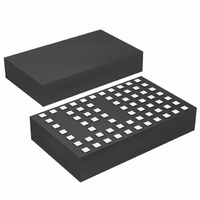
LTM4608AMPV#PBF Linear Technology, LTM4608AMPV#PBF Datasheet - Page 20

LTM4608AMPV#PBF
Manufacturer Part Number
LTM4608AMPV#PBF
Description
IC BUCK SYNC ADJ 8A 68LGA
Manufacturer
Linear Technology
Series
µModuler
Type
Point of Load (POL) Non-Isolatedr
Datasheet
1.LTM4608AEVPBF.pdf
(26 pages)
Specifications of LTM4608AMPV#PBF
Output
0.6 ~ 5 V
Number Of Outputs
1
Power (watts)
40W
Mounting Type
Surface Mount
Voltage - Input
2.7 ~ 5.5 V
Package / Case
68-LGA
1st Output
0.6 ~ 5 VDC @ 8A
Size / Dimension
0.59" L x 0.35" W x 0.11" H (15mm x 9mm x 2.8mm)
Power (watts) - Rated
40W
Operating Temperature
-55°C ~ 125°C
Efficiency
95%
Lead Free Status / RoHS Status
Lead free / RoHS Compliant
3rd Output
-
2nd Output
-
Available stocks
Company
Part Number
Manufacturer
Quantity
Price
LTM4608A
APPLICATIONS INFORMATION
Safety Considerations
The LTM4608A modules do not provide isolation from V
to V
fuse with a rating twice the maximum input current needs
to be provided to protect each unit from catastrophic failure.
Layout Checklist/Example
The high integration of LTM4608A makes the PCB board
layout very simple and easy. However, to optimize its
electrical and thermal performance, some layout con-
siderations are still necessary.
• Use large PCB copper areas for high current path,
20
including V
PCB conduction loss and thermal stress.
OUT
. There is no internal fuse. If required, a slow blow
IN
, GND and V
OUT
. It helps to minimize the
C
GND
IN
C
V
IN
IN
Figure 17. Recommended PCB Layout
IN
GND
• Place high frequency ceramic input and output capaci-
• Place a dedicated power ground layer underneath the
• To minimize the via conduction loss and reduce module
• Do not put vias directly on the pads, unless they are
• Use a separated SGND ground copper area for com-
Figure 17 gives a good example of the recommended layout.
tors next to the V
high frequency noise.
unit.
thermal stress, use multiple vias for interconnection
between top layer and other power layers.
capped.
ponents connected to signal pins. Connect the SGND
to GND underneath the unit.
V
C
C
C
GND
4608A F17
OUT
OUT
OUT
OUT
IN
, GND and V
OUT
pins to minimize
4608afc


