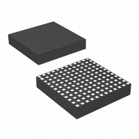
LTM4616IV#PBF Linear Technology, LTM4616IV#PBF Datasheet - Page 12

LTM4616IV#PBF
Manufacturer Part Number
LTM4616IV#PBF
Description
IC DC/DC UMODULE DUAL 8A 144-LGA
Manufacturer
Linear Technology
Series
µModuler
Type
Point of Load (POL) Non-Isolatedr
Datasheet
1.LTM4616EVPBF.pdf
(28 pages)
Specifications of LTM4616IV#PBF
Design Resources
LTM4616 Spice Model
Output
0.6 ~ 5 V
Number Of Outputs
2
Power (watts)
12W
Mounting Type
Surface Mount
Voltage - Input
2.7 ~ 5.5 V
Package / Case
144-LGA
1st Output
0.6 ~ 5 VDC @ 8A
2nd Output
0.6 ~ 5 VDC @ 8A
Size / Dimension
0.59" L x 0.59" W x 0.11" H (15mm x 15mm x 2.8mm)
Power (watts) - Rated
12W
Operating Temperature
-40°C ~ 125°C
Lead Free Status / RoHS Status
Lead free / RoHS Compliant
3rd Output
-
Available stocks
Company
Part Number
Manufacturer
Quantity
Price
LTM4616
applications inForMation
peak current value in normal operation even though the
voltage at the I
at the I
is greater than the load requirement. As the I
drops below 0.2V, the BURST comparator trips, causing
the internal sleep line to go high and turn off both power
MOSFETs.
In Burst Mode operation, the internal circuitry is partially
turned off, reducing the quiescent current to about 450µA
for each output. The load current is now being supplied
from the output capacitors. When the output voltage drops,
causing I
low, and the LTM4616 resumes normal operation. The next
oscillator cycle will turn on the top power MOSFET and the
switching cycle repeats. Each regulator can be configured
for Burst Mode operation.
Pulse-Skipping Mode Operation
In applications where low output ripple and high efficiency
at intermediate currents are desired, pulse-skipping mode
should be used. Pulse-skipping operation allows the
LTM4616 to skip cycles at low output loads, thus increasing
efficiency by reducing switching loss. Floating the MODE
pin or tying it to V
This allows discontinuous conduction mode (DCM) opera-
tion down to near the limit defined by the chip’s minimum
on-time (about 100ns). Below this output current level,
the converter will begin to skip cycles in order to main-
tain output regulation. Increasing the output load current
slightly, above the minimum required for discontinuous
conduction mode, allows constant frequency PWM. Each
regulator can be configured for pulse-skipping mode.
Forced Continuous Operation
In applications where fixed frequency operation is more
critical than low current efficiency, and where the lowest
output ripple is desired, forced continuous operation should
be used. Forced continuous operation can be enabled by
tying the MODE pin to GND. In this mode, inductor cur-
rent is allowed to reverse during low output loads, the I
voltage is in control of the current comparator threshold
12
TH
TH
pin drops when the inductor’s average current
to rise above 0.25V, the internal sleep line goes
TH
pin indicates a lower value. The voltage
IN
/2 enables pulse-skipping operation.
TH
voltage
TH
throughout, and the top MOSFET always turns on with
each oscillator pulse. During start-up, forced continu-
ous mode is disabled and inductor current is prevented
from reversing until the LTM4616’s output voltage is in
regulation. Each regulator can be configured for forced
continuous mode.
Multiphase Operation
For output loads that demand more than 8A of current,
two outputs in LTM4616 or even multiple LTM4616s can
be cascaded to run out-of-phase to provide more output
current without increasing input and output voltage ripple.
The CLKIN pin allows the LTC4616 to synchronize to an
external clock (between 0.75MHz and 2.25MHz) and the
internal phase-locked loop allows the LTM4616 to lock
onto CLKIN’s phase as well. The CLKOUT signal can be
connected to the CLKIN pin of the following LTM4616 stage
to line up both the frequency and the phase of the entire
system. Tying the PHMODE pin to SV
(floating) generates a phase difference (between CLKIN
and CLKOUT) of 180°, 120° or 90° respectively, which
corresponds to a 2-phase, 3-phase or 4-phase operation.
For a 6-phase example in Figure 2, the 2nd stage that is
120° out-of-phase from the 1st stage can generate a 240°
(PHMODE = 0) CLKOUT signal for the 3rd stage, which
then can generate a CLKOUT signal that’s 420°, or 60°
(PHMODE = SV
input, the next two stages can shift 120° (PHMODE = 0)
for each to generate a 300° signal for the 6th stage. Finally,
the signal with a 60° phase shift on the 6th stage (PHMODE
is floating) goes back to the 1st stage. Figure 3 shows the
configuration for 12-phase operation.
A multiphase power supply significantly reduces the
amount of ripple current in both the input and output
capacitors. The RMS input ripple current is reduced by,
and the effective ripple frequency is multiplied by, the
number of phases used (assuming that the input voltage
is greater than the number of phases used times the output
voltage). The output ripple amplitude is also reduced by
the number of phases used.
IN
) for the 4th stage. With the 60° CLKIN
IN
, SGND or SV
4616fc
IN
/2


