LTM4619IV#PBF Linear Technology, LTM4619IV#PBF Datasheet
LTM4619IV#PBF
Specifications of LTM4619IV#PBF
Available stocks


Related parts for LTM4619IV#PBF


LTM4619IV#PBF Summary of contents
Page 1
... ATCA Cards n Industrial Equipment n Point of Load Regulation L, LT, LTC, LTM, Linear Technology, the Linear logo, Burst Mode and μModule are registered trademarks of Linear Technology Corporation. All other trademarks are the property of their respective owners. TYPICAL APPLICATION Dual 4A 3.3V/2.5V DC/DC μModule MODE/PLLIN INTV 5 ...
Page 2
... LTM4619EV#PBF LTM4619EV#PBF LTM4619IV#PBF LTM4619IV#PBF Consult LTC Marketing for parts specifi ed with wider operating temperature ranges. *The temperature grade is identifi label on the shipping container. For more information on lead free part marking, go to: This product is only offered in trays. For more information go to: ELECTRICAL CHARACTERISTICS operating temperature range, otherwise specifi ...
Page 3
ELECTRICAL CHARACTERISTICS operating temperature range, otherwise specifi cations are at T each channel (Note 3). SYMBOL PARAMETER I Input Inrush Current at Start-Up INRUSH(VIN) I Input Supply Bias Current Q(VIN) I Input Supply Current S(VIN) INTV Internal V Voltage CC ...
Page 4
LTM4619 ELECTRICAL CHARACTERISTICS operating temperature range, otherwise specifi cations are at T each channel. (Note 3) SYMBOL PARAMETER f Nominal Frequency NOM f Lowest Frequency LOW f Highest Frequency HIGH R MODE/PLLIN Input Resistance MODE/PLLIN I Frequency Setting FREQ Sinking ...
Page 5
TYPICAL PERFORMANCE CHARACTERISTICS 1.2V Output Transient Response I OUT 1A/DIV V OUT 50mV/DIV 100μs/DIV 4619 G04 6V 1.2V AT 2A/μs LOAD STEP IN OUT f = 780kHz C 2 22μF, 6.3V X5R CERAMIC OUT C 1 330μF, 6.3V SANYO POSCAP ...
Page 6
LTM4619 PIN FUNCTIONS V (J1 to J3, J10 to J12 K4 K12 L5 L12 M12): Power Input Pins. Apply input voltage between these pins and PGND pins. Recommend placing ...
Page 7
SIMPLIFIED BLOCK DIAGRAM INTV CC PGOOD MODE/PLLIN EXTV TK/SS1 C SS1 R1 RUN1 COMP1 R2 R2 • TK/SS2 = UVLO THRESHOLD = 1.22V C SS2 RUN2 COMP2 FREQ SGND DECOUPLING REQUIREMENTS SYMBOL PARAMETER ...
Page 8
... TK/SS pin is used for programming the output voltage ramp and voltage tracking during start-up. See the Applications Information section. The LTM4619 is internally compensated to be stable over all operating conditions. The Linear Technology μModule Power Design Tool will be provided for transient and stability analysis. The V pin is used to program the FB output voltage with a single external resistor to ground ...
Page 9
... Additional output fi ltering may be required by the system designer, if further reduction of output ripples or dynamic transient spikes is required. The Linear Technology μModule Power Design Tool will be provided for stability analysis. Multiphase operation will reduce effective output ripple as a function of the number of phases ...
Page 10
LTM4619 APPLICATIONS INFORMATION Mode Selections and Phase-Locked Loop The LTM4619 can be enabled to enter high effi ciency Burst Mode operation, constant-frequency pulse-skipping mode, or forced continuous conduction mode. To select the forced continuous operation, tie the MODE/PLLIN pin to ...
Page 11
APPLICATIONS INFORMATION Soft-Start and Tracking The LTM4619 has the ability to either soft-start by itself with a capacitor or track the output of another channel or external supply. When one particular channel is confi gured to soft-start by itself, a ...
Page 12
LTM4619 APPLICATIONS INFORMATION 0.60 0.55 0.50 0.45 0.40 0.35 0.30 0.25 0.20 0.15 0.10 0.05 0 0.1 0.15 0.2 0.25 0.3 0.35 0.4 0.45 0.5 0.55 0.6 0.65 0.7 0.75 0.8 0.85 0.9 Figure 5. Normalized Input RMS Ripple Current ...
Page 13
APPLICATIONS INFORMATION Multiphase Operation Multiphase operation with multiple LTM4619 devices in parallel will lower the effective input RMS ripple current as well as the output ripple current due to the interleaving operation of the regulators. Figure 5 provides a ratio ...
Page 14
... CC device temperature rise. Slope Compensation The module has already been internally compensated for all output voltages. The Linear Technology μModule Power Design Tool will be provided for control loop op- timization. Burst Mode Operation and Pulse-Skipping Mode The LTM4619 regulator can be placed into high effi ciency power saving modes at light load condition to conserve power. The Burst Mode operation can be selected by fl ...
Page 15
APPLICATIONS INFORMATION Table 2. 1.5V Output DERATING CURVE V (V) IN Figures Figures Figures Figures 10 Figures 10 Figures 10 ...
Page 16
LTM4619 APPLICATIONS INFORMATION AMBIENT TEMPERATURE (°C) Figure 9. 6V without Heat Sink ...
Page 17
APPLICATIONS INFORMATION Layout Checklist/Example The high integration of LTM4619 makes the PCB board layout very simple and easy. However, to optimize its electri- cal and thermal performance, some layout considerations are still necessary. • Use large PCB copper areas for ...
Page 18
LTM4619 TYPICAL APPLICATIONS V IN 4.5V TO 26. 10μ OUT1 5V/4A C OUT1 100μF INTV Figure 18. Typical 4.5V to 26.5V Input, 5V and 3.3V Outputs at 4A Design 18 MODE/PLLIN INTV CC V FREQ/PLLFLTR IN ...
Page 19
TYPICAL APPLICATIONS 26.5V 10μ OUT1 1.2V/4A C OUT1 100μF 2 INTV Figure 19. Typical 4.5V to 26.5V Input, 1.2V and 1.5V Outputs at 4A Design with Adjusted Frequency at 500kHz MODE/PLLIN INTV ...
Page 20
LTM4619 TYPICAL APPLICATIONS 26.5V Figure 20. Output Paralleled LTM4619 Module for 5V Output at 8A Design 20 MODE/PLLIN EXTV INTV FREQ/PLLFLTR COMP1 V 10μF FB1 COMP2 V FB2 TK/SS1 V ...
Page 21
TYPICAL APPLICATIONS 26. IN2 IN1 10μF 330μ OUT1 5V/ 220μF 2 PHASE OSCILLATOR + V OUT1 C3 GND OUT2 LTC6908-2 R9 0.1μF SET MOD 143k V OUT3 2.5V/4A + ...
Page 22
LTM4619 PACKAGE DESCRIPTION PIN NAME A1 V OUT2 A2 V OUT2 A3 V OUT2 A4 GND A5 GND A6 GND A7 GND A8 GND A9 GND A10 V OUT1 A11 V OUT1 A12 V OUT1 B1 V OUT2 B2 V ...
Page 23
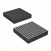
... PACKAGE DESCRIPTION Information furnished by Linear Technology Corporation is believed to be accurate and reliable. However, no responsibility is assumed for its use. Linear Technology Corporation makes no representa- tion that the interconnection of its circuits as described herein will not infringe on existing patent rights. LGA Package 144-Lead (15mm × 15mm × 2.82mm) ...
Page 24
... Two 4A Outputs and One 1.5A; 15mm × 15mm × 2.8mm LGA ≤ 5V; 15mm × 15mm × 2.8mm LGA 2.7V ≤ V ≤ 5.5V; 0.6V ≤ OUT www.linear.com ● ≤ 5V; 15mm × 15mm × 2.8mm LGA LT 0709 • PRINTED IN USA © LINEAR TECHNOLOGY CORPORATION 2009 4619f ...