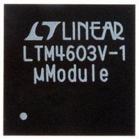
LTM4603EV-1#PBF Linear Technology, LTM4603EV-1#PBF Datasheet - Page 8

LTM4603EV-1#PBF
Manufacturer Part Number
LTM4603EV-1#PBF
Description
IC DC/DC UMODULE 6A 118-LGA
Manufacturer
Linear Technology
Series
µModuler
Type
Point of Load (POL) Non-Isolatedr
Datasheet
1.LTM4603EV-1PBF.pdf
(24 pages)
Specifications of LTM4603EV-1#PBF
Design Resources
LTM4603-1 Spice Model
Output
0.6 ~ 5 V
Number Of Outputs
1
Power (watts)
30W
Mounting Type
Surface Mount
Voltage - Input
4.5 ~ 20V
Package / Case
118-LGA
1st Output
0.6 ~ 5 VDC @ 6A
Size / Dimension
0.59" L x 0.59" W x 0.11" H (15mm x 15mm x 2.8mm)
Power (watts) - Rated
30W
Operating Temperature
-40°C ~ 85°C
Efficiency
93%
Lead Free Status / RoHS Status
Lead free / RoHS Compliant
3rd Output
-
2nd Output
-
Available stocks
Company
Part Number
Manufacturer
Quantity
Price
LTM4603/LTM4603-1
MARG0 (Pin C12): This pin is the LSB logic input for the
margining function. Together with the MARG1 pin will
determine if margin high, margin low or no margin state
is applied. The pin has an internal pull-down resistor of
50k. See Applications Information.
MARG1 (Pin D12): This pin is the MSB logic input for the
margining function. Together with the MARG0 pin will
determine if margin high, margin low or no margin state
is applied. The pin has an internal pull-down resistor of
50k. See Applications Information.
SGND (Pin H12): Signal Ground. This pin connects to
PGND at output capacitor point.
COMP (Pin A11): Current Control Threshold and Error
Amplifi er Compensation Point. The current comparator
threshold increases with this control voltage. The voltage
ranges from 0V to 2.4V with 0.7V corresponding to zero
sense voltage (zero current).
PIN FUNCTIONS
SIMPLIFIED BLOCK DIAGRAM
8
FUNCTION
UVLO
V
IN
R1
R2
C
40.2k
>1.9V = ON
SS
<1V = OFF
MAX = 5V
R
FB
TRACK/SS
V
OUT_LCL
MARG1
MARG0
PGOOD
INTV
MPGM
DRV
COMP
PLLIN
SGND
(See Package Description for Pin Assignment)
RUN
f
V
SET
CC
CC
FB
Figure 1. Simplifi ed LTM4603/LTM4603-1 Block Diagram
INTERNAL
COMP
33.2k
4.7μF
60.4k
(50Ω, LTM4603-1)
50k
POWER CONTROL
1M
50k
50k
V
OUT
5.1V
ZENER
PGOOD (Pin G12): Output Voltage Power Good Indicator.
Open-drain logic output that is pulled to ground when the
output voltage is not within ±10% of the regulation point,
after a 25μs power bad mask timer expires.
RUN (Pin A10): Run Control Pin. A voltage above 1.9V
will turn on the module, and when below 1V, will turn off
the module. A programmable UVLO function can be ac-
complished with a resistor from V
5.1V zener to ground. Maximum pin voltage is 5V. Limit
current into the RUN pin to less than 1mA.
V
to bypass the remote sense amplifi er, or DIFFV
nects to this pin when remote sense amplifi er is used.
V
V
the LTM4603-1.
OUT_LCL
OUT_LCL
OUT
is internally connected to V
10k
can be connected to V
(Pin L12): V
INTV
CC
–
+
Q1
Q2
10k
10k
22μF
1.5μF
OUT
10k
connects directly to this pin
PGND
V
V
DIFFV
C
+
OSNS
OSNS
OUT
4603 F01
OUT
+
–
+
OUT_LCL
C
OUT
IN
IN
V
4.5V TO 20V
V
1.5V
6A
to this pin that has a
IN
OUT
on the LTM4603-1.
NOT INCLUDED
IN THE LTM4603-1
V
V
DIFFV
OSNS –
OSNS +
through 50Ω in
OUT
= NC1
= NC2
= NC3
OUT
con-
4603fa


