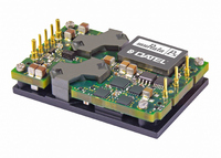
UQQ-3.3/25-Q48NB-C Murata Power Solutions Inc, UQQ-3.3/25-Q48NB-C Datasheet - Page 13

UQQ-3.3/25-Q48NB-C
Manufacturer Part Number
UQQ-3.3/25-Q48NB-C
Description
CONV DC/DC 82.5W 25A 3.3V T/H
Manufacturer
Murata Power Solutions Inc
Series
UQQr
Type
Isolatedr
Datasheet
1.UQQ-128-Q12PB-C.pdf
(18 pages)
Specifications of UQQ-3.3/25-Q48NB-C
Output
3.3V
Number Of Outputs
1
Power (watts)
82W
Mounting Type
Through Hole
Voltage - Input
18 ~ 75V
Package / Case
8-DIP Module, 1/4 Brick
1st Output
3.3 VDC @ 25A
Size / Dimension
2.22" L x 1.45" W x 0.50" H (56.4mm x 36.8mm x 12.7mm)
Power (watts) - Rated
82.5W
Operating Temperature
-40°C ~ 85°C
Efficiency
88%
Approvals
CSA, cUL, EN, UL
Output Type
Quarter-Brick
No. Of Output Channels
1
Input Voltage
18V To 75V
Power Rating
82.5W
Output Voltage
3.3V
Output Current
25A
Supply Voltage
48V
Dc / Dc Converter Case
RoHS Compliant
Dc / Dc Converter O/p Type
Quarter-Brick
No. Of Outputs
1
Rohs Compliant
Yes
Product
Isolated
Output Power
83 W
Input Voltage Range
18 V to 75 V
Input Voltage (nominal)
48 V
Output Voltage (channel 1)
3.3 V
Output Current (channel 1)
25 A
Isolation Voltage
2.25 KV
Package / Case Size
Quarter Brick
Lead Free Status / RoHS Status
Lead free / RoHS Compliant
3rd Output
-
2nd Output
-
4th Output
-
Lead Free Status / Rohs Status
Details
Other names
811-1891-5
Available stocks
Company
Part Number
Manufacturer
Quantity
Price
Part Number:
UQQ-3.3/25-Q48NB-C
Manufacturer:
MURATA/村田
Quantity:
20 000
Soldering Guidelines
Murata Power Solutions recommends the specifi cations below when installing these
converters. These specifi cations vary depending on the solder type. Exceeding these
specifi cations may cause damage to the product. Your production environment may dif-
fer; therefore please thoroughly review these guidelines with your process engineers.
Removal of Soldered UQQ’s from Printed Circuit Boards
Should removal of the UQQ from its soldered connection be needed, thor-
oughly de-solder the pins using solder wicks or de-soldering tools. At no time
should any prying or leverage be used to remove boards that have not been
properly de-soldered fi rst.
Input Source Impedance
UQQ converters must be driven from a low ac-impedance input source. The
DC/DC’s performance and stability can be compromised by the use of highly
inductive source impedances. The input circuit shown in Figure 2 is a practical
solution that can be used to minimize the effects of inductance in the input
traces. For optimum performance, components should be mounted close to the
DC/DC converter.
I/O Filtering, Input Ripple Current, and Output Noise
All models in the UQQ Series are tested/specifi ed for input ripple current (also
called input refl ected ripple current) and output noise using the circuits and
layout shown in Figures 2 and 3. External input capacitors (C
serve primarily as energy-storage elements.
For Sn/Ag/Cu based solders:
Maximum Preheat Temperature
Maximum Pot Temperature
Maximum Solder Dwell Time
Technical Notes
Wave Solder Operations for through-hole mounted products (THMT)
V
OSCILLOSCOPE
IN
+
–
C
C
L
TO
BUS
IN
BUS
= 33μF, ESR < 700mΩ @ 100kHz
= 12μH
= 220μF, ESR < 100mΩ @ 100kHz
Figure 2. Measuring Input Ripple Current
C
BUS
L
BUS
115° C.
270° C.
7 seconds
CURRENT
PROBE
C
IN
For Sn/Pb based solders:
Maximum Preheat Temperature
Maximum Pot Temperature
Maximum Solder Dwell Time
3
1
+INPUT
–INPUT
IN
in Figure 2)
www.murata-ps.com
105° C.
250° C.
6 seconds
They should be selected for bulk capacitance (at appropriate frequencies),
low ESR, and high rms-ripple-current ratings. The switching nature of
DC/DC converters requires that dc voltage sources have low ac impedance as
highly inductive source impedance can affect system stability. In Figure 2,
C
fi guration may necessitate additional considerations.
In critical applications, output ripple/noise (also referred to as periodic
and random deviations or PARD) can be reduced below specifi ed limits
using fi ltering techniques, the simplest of which is the installation of
additional external output capacitors. Output capacitors function as true
fi lter elements and should be selected for bulk capacitance, low ESR, and
appropriate frequency response. In Figure 3, the two copper strips simulate
real-world pcb impedances between the power supply and its load. Scope
measurements should be made using BNC connectors or the probe ground
should be less than ½ inch and soldered directly to the fi xture.
All external capacitors should have appropriate voltage ratings and be
located as close to the converter as possible. Temperature variations for all
relevant parameters should be taken into consideration. OS-CON
semiconductor capacitors (www.sanyo.com) can be especially effective for
further reduction of ripple/noise. The most effective combination of external
I/O capacitors will be a function of line voltage and source impedance, as
well as particular load and layout conditions.
Wide Input Range Single Output DC/DC Converters
BUS
and L
BUS
+OUTPUT
–OUTPUT
+SENSE
simulate a typical dc voltage bus. Your specifi c system con-
–SENSE
Figure 3. Measuring Output Ripple/Noise (PARD)
C1 = 1μF CERAMIC
C2 = 10μF TANTALUM
LOAD 2-3 INCHES (51-76mm) FROM MODULE
7
8
4
5
C1
COPPER STRIP
COPPER STRIP
25 Mar 2011 MDC_UQQ.B01 Page 13 of 18
C2
email: sales@murata-ps.com
UQQ Series
SCOPE
TM
R
LOAD
organic


