591-2404-013F Dialight, 591-2404-013F Datasheet - Page 5
591-2404-013F
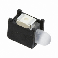
Manufacturer Part Number
591-2404-013F
Description
LED YELLOW PRISM/CBI 587NM SMD
Manufacturer
Dialight
Series
Prism®, CBI®r
Specifications of 591-2404-013F
Color
Yellow
Voltage Rating
1.8V
Current
20mA
Lens Style/size
Round, 2.84mm
Configuration
Single
Mounting Type
Surface Mount
Lead Free Status / RoHS Status
Lead free / RoHS Compliant
Lens Type
-
Other names
350-2315-2


Pin Definitions
Note
Document Number: 001-57344 Rev. *A
Pin Name
DQ
LD
BWS
BWS
BWS
BWS
A
R/W
QVLD
ODT
K
K
CQ
CQ
ZQ
DOFF
3. On-Die Termination (ODT) feature is supported for D
[35:0]
0
1
2
3
[3]
,
,
,
Input Output-
Synchronous
Synchronous
Synchronous
Synchronous
Synchronous
Valid output
Termination
Echo Clock
Echo Clock
Input Clock
Input Clock
indicator
input pin
On-Die
Input-
Input-
Input-
Input-
Input
Input
I/O
Data Input Output Signals. Inputs are sampled on the rising edge of K and K clocks during valid write
operations. These pins drive out the requested data when the read operation is active. Valid data is driven
out on the rising edge of both the K and K clocks during read operations. When read access is deselected,
DQ
Synchronous Load. Sampled on the rising edge of the K clock. This input is brought LOW when a bus
cycle sequence is defined. This definition includes address and read/write direction. All transactions
operate on a burst of 2 data. LD must meet the setup and hold times around edge of K.
Byte Write Select 0, 1, 2, and 3 − Active LOW. Sampled on the rising edge of the K and K clocks during
write operations. Used to select which byte is written into the device during the current portion of the write
operations. Bytes not written remain unaltered. BWS
controls D
All the Byte Write Selects are sampled on the same edge as the data. Deselecting a Byte Write Select
ignores the corresponding byte of data and it is not written into the device.
Address Inputs. Sampled on the rising edge of the K clock during active read and write operations. These
address inputs are multiplexed for both read and write operations. Internally, the device is organized as
512K x 36 (2 arrays each of 256K x 36).
Synchronous Read or Write Input. When LD is LOW, this input designates the access type (read when
R/W is HIGH, write when R/W is LOW) for loaded address. R/W must meet the setup and hold times
around edge of K.
Valid Output Indicator. The Q Valid indicates valid output data. QVLD is edge aligned with CQ and CQ.
On-Die Termination Input. This pin is used for On-Die termination of the input signals. ODT range
selection is made during power up initialization. A LOW on this pin selects a low range that follows RQ/3.33
for 175Ω < RQ < 350Ω (where RQ is the resistor tied to ZQ pin). A HIGH on this pin selects a high range
that follows RQ/1.66 for 175Ω < RQ < 250Ω (where RQ is the resistor tied to ZQ pin). When left floating,
a high range termination value is selected by default.
Positive Input Clock Input. The rising edge of K is used to capture synchronous inputs to the device
and to drive out data through Q
Negative Input Clock Input. K is used to capture synchronous data being presented to the device and
to drive out data through Q
Synchronous Echo Clock Outputs. This is a free running clock and is synchronized to the input clock
(K) of the DDR II+. The timing for the echo clocks is shown in the
Synchronous Echo Clock Outputs. This is a free running clock and is synchronized to the input clock
(K) of the DDR II+. The timing for the echo clocks is shown in the
Output Impedance Matching Input. This input is used to tune the device outputs to the system data bus
impedance. CQ, CQ, and Q
between ZQ and ground. Alternatively, this pin can be connected directly to V
minimum impedance mode. This pin cannot be connected directly to GND or left unconnected.
PLL Turn Off − Active LOW. Connecting this pin to ground turns off the PLL inside the device. The timing
in the PLL turned off operation differs from those listed in this data sheet. For normal operation, this pin
can be connected to a pull up through a 10 KΩ or less pull up resistor. The device behaves in DDR I mode
when the PLL is turned off. In this mode, the device can be operated at a frequency of up to 167 MHz
with DDR I timing.
[35:0]
are automatically tri-stated.
[26:18]
and BWS
[x:0]
, BWS
[x:0]
3
[x:0]
, and K/K inputs.
controls D
[x:0]
.
[x:0]
output impedance are set to 0.2 x RQ, where RQ is a resistor connected
. All accesses are initiated on the rising edge of K.
[35:27]
.
Pin Description
0
controls D
[8:0]
Switching Characteristics
Switching Characteristics
, BWS
1
CY7C21701KV18
controls D
DDQ
, which enables the
[17:9]
, BWS
Page 5 of 24
on page 21.
on page 21.
2
[+] Feedback
Related parts for 591-2404-013F
Image
Part Number
Description
Manufacturer
Datasheet
Request
R

Part Number:
Description:
LED PRISM 3MM RND LC SQ YLW SMD
Manufacturer:
Dialight
Datasheet:
Part Number:
Description:
LED PRISM 3MM RND LC YLW SMD
Manufacturer:
Dialight
Datasheet:
Part Number:
Description:
LED PRISM 3MM RND LC SQ YLW SMD
Manufacturer:
Dialight
Datasheet:
Part Number:
Description:
LED PRISM 3MM RND LC YLW SMD
Manufacturer:
Dialight
Datasheet:
Part Number:
Description:
LED PRISM 3MM RND LC SQ YLW SMD
Manufacturer:
Dialight
Datasheet:

Part Number:
Description:
LED PRISM 3MM GREEN
Manufacturer:
Dialight
Datasheet:

Part Number:
Description:
LED PRISM 3MM RT ANG YELLOW SMT
Manufacturer:
Dialight
Datasheet:

Part Number:
Description:
LED PRISM 3MM RT ANG GREEN SMT
Manufacturer:
Dialight
Datasheet:
Part Number:
Description:
LED PRISM 3MM RA HIEFF RED SMT
Manufacturer:
Dialight
Datasheet:
Part Number:
Description:
LED PRISM 3MM ALGASS RED SMT
Manufacturer:
Dialight
Datasheet:
Part Number:
Description:
LED PRISM 3MM RA ALGAAS RED SMT
Manufacturer:
Dialight
Datasheet:

Part Number:
Description:
LED PRISM 3MM RA SUP RED/GRN SMT
Manufacturer:
Dialight
Datasheet:
Part Number:
Description:
LED PRISM 3MM RT ANG YEL/GRN SMT
Manufacturer:
Dialight
Datasheet:
Part Number:
Description:
LED 3MM PRISM BLUE SMD
Manufacturer:
Dialight
Datasheet: