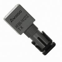
HFBR-1412TZ Avago Technologies US Inc., HFBR-1412TZ Datasheet - Page 20
HFBR-1412TZ
Manufacturer Part Number
HFBR-1412TZ
Description
XMITTER FIBER OPTIC STD PWR ST
Manufacturer
Avago Technologies US Inc.
Specifications of HFBR-1412TZ
Wavelength
820nm
Voltage - Forward (vf) Typ
1.7V
Current - Dc Forward (if)
100mA
Voltage - Dc Reverse (vr) (max)
1.8V
Capacitance
55pF
Connector Type
ST
Function
High performance fiber optic communication links for information systems and industrial applications.
Product
Transmitter
Data Rate
5 MBd
Diode Capacitance
55 pF
Maximum Rise Time
6.5 ns
Maximum Fall Time
6.5 ns
Pulse Width Distortion
7.56 ns
Maximum Output Current
25 mA
Operating Supply Voltage
4.75 V to 5.25 V
Maximum Operating Temperature
+ 85 C
Minimum Operating Temperature
- 40 C
Lead Free Status / RoHS Status
Lead free / RoHS Compliant
Spectral Bandwidth
-
Lead Free Status / Rohs Status
Lead free / RoHS Compliant
For Use With
Multimode Glass, Hard Clad Silica
Lead Free Status / RoHS Status
Lead free / RoHS Compliant, Lead free / RoHS Compliant
Other names
516-2036


HFBR-24x2Z Low-Cost 5 MBd Receiver
Description
The HFBR-24x2Z fiber optic receiver is designed to oper-
ate with the Avago Technologies HFBR-14xxZ fiber optic
transmitter and 50/125 μm, 62.5/125 μm, 100/ 140 μm,
and 200 μm HCS® fiber optic cable. Consistent coupling
into the receiver is assured by the lensed optical system
(Figure 1). Response does not vary with fiber size d 0.100
μm.
The HFBR-24x2Z receiver incorporates an integrated
photo IC containing a photodetector and dc amplifier
driving an opencollector Schottky output transistor. The
HFBR-24x2Z is designed for direct interfacing to popular
logic families. The absence of an internal pull-up resistor
allows the open-collector output to be used with logic
families such as CMOS requiring voltage excursions much
higher than V
Both the open-collector “Data” output Pin 6 and V
are referenced to “Com” Pin 3, 7. The “Data” output allows
busing, strobing and wired “OR” circuit configurations.
The transmitter is designed to operate from a single +5
V supply. It is essential that a bypass capacitor (0.1 mF
ceramic) be connected from Pin 2 (V
common) of the receiver.
Absolute Maximum Ratings
20
Parameter
Storage Temperature
Operating Temperature
Lead Soldering Cycle
Supply Voltage
Output Current
Output Voltage
Output Collector Power Dissipation
Fan Out (TTL)
Temp
Time
CC
.
CC
Symbol
T
T
V
I
V
P
N
O
) to Pin 3 (circuit
A
S
CC
O
O AV
CC
Pin 2
Min
-55
-40
-0.5
-0.5
Housed Product
BOTTOM VIEW
NOTES:
1. PINS 1, 4, 5 AND 8 ARE ELECTRICALLY CONNECTED.
2. PINS 3 AND 7 ARE ELECTRICALLY CONNECTED TO THE HEADER.
Max
+85
+85
+260
10
7.0
25
18.0
40
5
4 5
3
2
1
6
7
8
Units
°C
°C
°C
sec
V
mA
V
mW
PIN 1 INDICATOR
2
6
7 & 3
V
DATA
COMMON
cc
Reference
Note 1
Note 2
PIN
1
3
4
5
7
8
2
6
1
2
1
1
2
1
FUNCTION
NC
V
COMMON
NC
NC
DATA
COMMON
NC
CC
(5 V)
Related parts for HFBR-1412TZ
Image
Part Number
Description
Manufacturer
Datasheet
Request
R

Part Number:
Description:
FIBER OPTIC CBL SIMPLEX 1=100M
Manufacturer:
Avago Technologies US Inc.
Datasheet:

Part Number:
Description:
FIBER OPTIC CBL SIMPLEX 1=500M
Manufacturer:
Avago Technologies US Inc.
Datasheet:

Part Number:
Description:
FIBER OPTIC CONN LATCH GRY SIMPL
Manufacturer:
Avago Technologies US Inc.
Datasheet:

Part Number:
Description:
FIBER OPTIC CONN LATCH BLU SIMPL
Manufacturer:
Avago Technologies US Inc.
Datasheet:

Part Number:
Description:
XMITTER VERSATILE LINK HORZ
Manufacturer:
Avago Technologies US Inc.
Datasheet:

Part Number:
Description:
Fiber Optic Transmitters, Receivers, Transceivers 1300nm 155MBd 16-pin DIP ST Rx
Manufacturer:
Avago Technologies US Inc.

Part Number:
Description:
FIBER OPTIC CBL DUPLEX 1=100M
Manufacturer:
Avago Technologies US Inc.
Datasheet:
Part Number:
Description:
FIBER OPTIC CBL SIMPLEX 1=500M
Manufacturer:
Avago Technologies US Inc.
Datasheet:
Part Number:
Description:
FIBER OPTIC CBL DUPLEX 1=500M
Manufacturer:
Avago Technologies US Inc.
Datasheet:

Part Number:
Description:
FIBER OPTIC CBL SIMPLEX 1=100M
Manufacturer:
Avago Technologies US Inc.
Datasheet:

Part Number:
Description:
OPTOCOUPLER GATE DRV 2A 16-SOIC
Manufacturer:
Avago Technologies US Inc.
Datasheet:
Part Number:
Description:
OPTOCOUPLER 2CH 2.5A 16-SOIC
Manufacturer:
Avago Technologies US Inc.
Datasheet:

Part Number:
Description:
OPTOCOUPLER GATE DRV 0.4A 16SOIC
Manufacturer:
Avago Technologies US Inc.
Datasheet:

Part Number:
Description:
OPTOCOUPLER 2.0A 250KHZ 8-DIP
Manufacturer:
Avago Technologies US Inc.
Datasheet:

Part Number:
Description:
OPTOCOUPLER 2.0A 250KHZ GW 8-SMD
Manufacturer:
Avago Technologies US Inc.
Datasheet: