M0220MD-202LDAR2 Newhaven Display, M0220MD-202LDAR2 Datasheet
M0220MD-202LDAR2
Specifications of M0220MD-202LDAR2


Related parts for M0220MD-202LDAR2


M0220MD-202LDAR2 Summary of contents
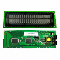
Page 1
... M0220MD‐202LDAR2 Vacuum Fluorescent Display Module RoHS Compliant ...
Page 2
... Digit Format 4.2 Outer Dimensions, Weight (See Fig_4 on page 5/11 for details) Parameter Outer Width Dimensions Height Thickness Weight DOCUMENT NO. M0220MD-202LDAR2 M0220MD-202LDAR2. M0220MD-202LDAR2 5*7 Dot Matrix with Descriptor Specification 193.0 1.0 64.0 1.0 25.0 Max Typical 220 REV.NO PAGE Table_1 Table_2 ...
Page 3
... Symbol Min. Typ. Vcc 4.5 5.0 3.5 Vih _ Vil ,Vcc=+5.0Vdc) Table_7 Symbol Min. Typ. Icc -- 800 Iih -1.0 -- Iil -1 100 200 DOCUMENT REV.NO NO M0220MD-202LDAR2 Table_3 Unit Table_4 Max. Unit +85 + Table_5 Max. Unit 5.5 Vdc 5.5 Vdc Table_6 Max. Unit 5.5 ...
Page 4
... AC Characteristics (Ta=+25 , Vcc=+5.0Vdc) Parameter CLK-DOUT Delay Time Delay Time Low to High Transit Time Low to High Delay time high to Low Transit Time High to Low 4.9 Timing Chart 4.9.1 Data Input Timing DOCUMENT NO. M0220MD-202LDAR2 Symbol Min. TYP. tPD -- -- tDLH -- 0.3 tTLH -- 2 ...
Page 5
... Signal Interfacing DOCUMENT M0220MD-202LDAR2 Driving Unit CLK DIN HVO1-HVO36 /CL LS ANODE VCC DRIVER GND VBB LS CLK /CL HVO1-HVO40 DIN VCC M0220MD-202LDAR2 GND VBB DC/DC Converter Circuit See Fig-4 on page See Fig-5 on page See Fig-9 on page REV.NO PAGE NO Display P1--P36 G1--G40 VFD 48-4001F F1 F2 ...
Page 6
... STANDARD NAME 32 -0.5 1.0 7.8 48.3 +0.7 1.0 17.5 (29.0) 0.5 56.0 1.0 4.0 1.0 64.0 DOCUMENT REV.NO NO. M0220MD-202LDAR2 00 10.0MAX 1.0 15.0 PAGE ...
Page 7
... STANDARD SPECIFICATION FOR APPROVAL NAME DOCUMENT REV.NO NO. M0220MD-202LDAR2 PAGE ...
Page 8
... Connector(Female): HIF3B-20D-2.54R (HIROSE) or equivalent Mate Socket (Male) BH-R20 FG (aster) or equivalent Pin Signal Pin No Vcc 2 GND 4 ANODE CLK 6 GND 8 GRID DATA 10 CLEAR 12 ANODE DATA 14 LATCH CLK 16 GND 18 Vcc 20 DOCUMENT REV.NO NO. M0220MD-202LDAR2 Table_9 Signal Vcc GND GND GND GND GND GND GND GND Vcc PAGE ...
Page 9
... The table below details the character position of the VFD Clock in the anode data Clock in the grid data Latch the anode and grid data Disable the clear signal Enable the clear signal TM bits is unused in the upper row DOCUMENT REV.NO NO. M0220MD-202LDAR2 00 (100H IS RECOMMANDED PAGE The ). ...
Page 10
... Avoid using the module where excessive noise interference is expected.Noise may affects the interface signal and causes improper operation. And it is important to keep the length of the interface cable less than 50cm. 6.11 Since all VFD modules contain C-MOS ICs,anti_static handling procedures are always required. DOCUMENT REV.NO NO. M0220MD-202LDAR2 00 PAGE ...
Page 11
... Temperature state) Duration:96hrs Vibration Frequency: 10 55Hz Displacement: 1.5mm Direction: Duration: 6hrs (2hrs for each direction) Condition: In unlighted state cycle DOCUMENT REV.NO NO. M0220MD-202LDAR2 00 Criteria Remarks Measurement shall be done Free of the after the Major specimens are Defects kept at room temperature for 24 hrs. PAGE ...
Page 12
... Newhaven Display reserves the right to change or modify the design of the VFD 8.2 module. Condition Criteria Time: 10ms Free of the Major Defects cycle 30min 5min 5min 30min DOCUMENT REV.NO NO. M0220MD-202LDAR2 Remarks Measurement shall be done after specimens kept at room temperature 24 hrs. PAGE the are ...