M0220SD-202SDAR1-1G Newhaven Display, M0220SD-202SDAR1-1G Datasheet
M0220SD-202SDAR1-1G
Specifications of M0220SD-202SDAR1-1G


Related parts for M0220SD-202SDAR1-1G


M0220SD-202SDAR1-1G Summary of contents
Page 1
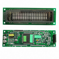
... M0220SD‐202SDAR1‐1G Vacuum Fluorescent Display Module RoHS Compliant protective PCB layout. Note additional 10K ohm resistors on IC input lines (R01 ~ R08). ...
Page 2
... The VFD used on the module is made of glass and should be handled with care. When handling the VFD recommended that cotton gloves be used. The module is equipped with a circuit protection fuse. Under no circumstances should the module be modified or repaired. Any unauthorized modifications or repairs will invalidate the product warranty. The module should be abolished as the factory waste. M0220SD-202SDAR1-1G ...
Page 3
... CGRAM ADDRESS SET 4-4-8. DDRAM ADDRESS SET 4-4-9. ADDRESS COUNTER READ 4-4-10. DDRAM OR CGRAM WRITE 4-4-11. DDRAM OR CGRAM READ 4-5. RESET CONDITIONS 5. CONNECTOR INTERFACE 6. JUMPER SETTING 7. CIRCUIT BLOCK DIAGRAM FIGURE-1 MECHANICAL DRAWING FIGURE-2 CHARACTER FONT TABLE 8. WARRANTY 9. OPERATING RECOMMENDATION PAGE M0220SD-202SDAR1-1G ...
Page 4
... Without condensation 20 90 %RH Without condensation Total amplitude: 1.5mm Freq: 10-55 Hz sine wave − Sweep time: 1 min./cycle Duration: 2hrs./axis (X,Y,Z) Duration: 11ms − Wave form: half sine wave 3 times/axis (X,Y,Z,-X,-Y,-Z) PAGE:1/19 Table-1 Typical 2 , 146 fL Table-2 Comment M0220SD-202SDAR1-1G ...
Page 5
... Vcc 140 Icc 0.7 0.7*Vcc Vcc-0 -500 I I Symbol Min. Max 230 EH PW 230 500 CYCLE t 160 DHR PAGE: 2/19 Table-3 Unit V V Table-4 Max. Unit 5.5 V 190 mA 1.045 W V Vcc 0.2* Vcc V V 0.5 V 1.0 A Table-5 Unit M0220SD-202SDAR1-1G ...
Page 6
... R DB0-DB7 Fig. 1. Motorola M68-Type Parallel Interface Write Cycle Timing R DB0-DB7 Fig. 2. Motorola M68-Type Parallel Interface Read Cycle Timing CYCLE DHR t CYCLE PAGE: 3/19 M0220SD-202SDAR1-1G ...
Page 7
... Fig. 3. Intel I80-Type Parallel Interface Write Cycle Timing Symbol Min RSS t 10 RSH WRL t 100 WRH t 30 DSi t 10 DHi t 166 CYCWR t 166 CYCRD t 70 RDL t 70 RDH t DDi t 5 DHRi t RSH WRH t WRL t OHi t DSi t CYCWR PAGE: 4/19 Table-6 Max. Unit M0220SD-202SDAR1-1G ...
Page 8
... Note: All timing is specified using 20% and 80% of Vcc as the reference points. t RSH RDH t RDL t t DDi DHRi t CYCRD Symbol Min. Max. t 100 STBS t 500 STBH 500 WSTB t 200 SCKH t 200 SCKL t 100 DSs t 100 DHs t 500 CYCSCK t 1 WAIT t DDs t 5 DHRs PAGE: 5/19 Table-7 Unit 150 ns ns M0220SD-202SDAR1-1G ...
Page 9
... STB t t CYCSCK STBS SCK t SCKL DSs SI Fig. 5. Synchronous Serial Interface Write Cycle Timing STB t t CYCSCK STBS SCK t SCKL DDs SI/SO Fig. 6. Synchronous Serial Interface Read Cycle Timing t SCKH DHs t SCKH DHs PAGE: 6/19 t WSTB t STBH t WSTB t STBH M0220SD-202SDAR1-1G ...
Page 10
... RSTL 4.5V t OFF IB7 IB3 BF= “0” IB6 IB2 IB6 IB5 IB1 IB5 IB4 IB0 IB4 Write Instruction Read Instruction PAGE:7/19 Table-8 Max. Unit RSTD IB3 IB7 IB3 IB2 IB6 IB2 IB1 IB5 IB1 IB0 IB4 IB0 Write Data M0220SD-202SDAR1-1G ...
Page 11
... SCK. Each read/write cycle begins on the falling edge of STB and ends on the rising edge valid read/write cycle, the STB must go high at the end of the cycle. IB7 BF=“0” IB6 IB6 IB0 IB0 Write Instruction Read Instruction PAGE: 8/19 DB7 DB6 DB0 Write Data M0220SD-202SDAR1-1G ...
Page 12
... Reset (RST/) input low “1” “0” R/W RS Instruction / Data “0” R/W RS Instruction / Data PAGE: 9/ M0220SD-202SDAR1-1G ...
Page 13
... DDRAM address and the character position on the VFD before and after a display shift (with the number of display lines set to 2). Relationship before a display shift (non-shifted Relationship after a display shift to the left Relationship after a display shift to the right PAGE: 10/19 M0220SD-202SDAR1-1G ...
Page 14
... DDRAM address set Address counter read DDRAM or CGRAM write DDRAM or CGRAM read x = don’t care CGRAM address R/W DB7 DB6 DB5 DB4 BF PAGE: 11/19 DB3 DB2 DB1 DB0 I S/C R BR1 BR0 CGRAM address DDRAM address AC contents Write data Read data M0220SD-202SDAR1-1G ...
Page 15
... DDRAM write. I The AC increments after each DDRAM or CGRAM access. If S=1, the information on the display shifts to the left by one character position after each DDRAM write The display shift function is disabled The display shift function is enabled I/D PAGE: 12/ M0220SD-202SDAR1-1G ...
Page 16
... DDRAM after this instruction. S/C R/L AC Contents (cursor position Decrements by one 0 1 Increments by one 1 0 Decrements by one 1 1 Increments by one row of pixels S/C R/L Information on the display No change No change Shifts on character position to the left Shifts on character position to the right PAGE: 13/19 B Table-10 M0220SD-202SDAR1-1G ...
Page 17
... E, WR/, and SCK cycle times specified in section 2.5 AC Timing Specifications. Due to this feature, the execution times for each instruction are not specified BR1 BR0 1 CG RAM Address DD RAM Address AC Contents PAGE: 14/19 M0220SD-202SDAR1-1G ...
Page 18
... The cursor is off The blinking character function is disabled. 6) Function Set instruction bits Sets the data bus width for the parallel interface modes to 8-bit (DB7-DB0 Number of display lines set to 2. BR1,BR0=0,0: Sets the luminance level to 100%. Write data Read data PAGE: 15/19 M0220SD-202SDAR1-1G ...
Page 19
... Note : JP3 JP7 must be set as shown above for either one of the parallel modes or for the serial mode. When the module is shipped , the parallel (Motorola) mode is set. M0220SD-202SDAR1-1G using Parallel Transfer mode. Jumper setting:J6 shorted and J2,J3,J5,J7 open. M0220SD-202SDAR1-S using Serial Data Transfer mode. Jumper setting:J3,J5,J6 shorted and J2,J7 open Pin NO ...
Page 20
... MECHANICAL DRAWING Connector: 2x7 Gold plated header, Molex P/N: 10-89-2141 or equivalent. Soldered onto backside of display. PAGE: 17/19 FIGURE-1 M0220SD-202SDAR1-1G ...
Page 21
... CHARACTER FONT TABLES RAM (1) CG RAM ( RAM (3) CG RAM ( RAM ( RAM (6) CG RAM ( RAM (8) CG RAM (1) CG RAM ( RAM (3) CG RAM ( RAM ( RAM (6) CG RAM ( RAM ( PAGE:18/19 FIGUER M0220SD-202SDAR1-1G ...
Page 22
... It is recommended to change the display patterns sometimes in order to keep best display quality. REMARKS This specification is subject to change without prior notice in order to improve the design and quality. Your consultation with Newhaven Display sales office is recommended for the use of this module. PAGE: 19/19 M0220SD-202SDAR1-1G ...