NHD-C12865BZ-FSW-GBW Newhaven Display, NHD-C12865BZ-FSW-GBW Datasheet - Page 4
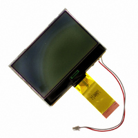
NHD-C12865BZ-FSW-GBW
Manufacturer Part Number
NHD-C12865BZ-FSW-GBW
Description
LCD COG GRAPH 128X65 WH TRANSFL
Manufacturer
Newhaven Display
Series
NHD-C12865BZ-Fr
Datasheet
1.NHD-C12865BZ-FSW-GBW.pdf
(12 pages)
Specifications of NHD-C12865BZ-FSW-GBW
Display Type
STN - Super-Twisted Nematic
Display Mode
Transflective
Viewing Area
60.10mm L x 34.50mm W
Backlight
LED - White
Dot Size
0.40mm W x 0.46mm H
Dot Pitch
0.44mm x 0.49mm
Dot Pixels
128 x 65
Pixel Density
128 x 65
Fluid Type
STN
Module Size (w X H X T)
66.3 mm x 49.8 mm x 5.9 mm
Backlighting
LED White
Operating Temperature Range
- 20 C to + 70 C
Product
Graphic LCD Module
Style
Chip-on-Glass (COG)
Lead Free Status / RoHS Status
Lead free / RoHS Compliant
Interface
-
Lead Free Status / Rohs Status
Lead free / RoHS Compliant
Available stocks
Company
Part Number
Manufacturer
Quantity
Price
Company:

Part Number:
NHD-C12865BZ-FSW-GBW
Manufacturer:
Newhaven Display
Quantity:
135


Pin Description and Wiring Diagram
Pin No. Symbol
Recommended LCD connector: 0.5mm pitch, 30 pin FFC. Molex p/n: 52892‐3095
Backlight connector: JST p/n: GHR‐02V‐S or equivalent Mates with: JST p/n: BM02B‐GHS‐TBT or SM02B‐GHS‐TB
10
11
12
13
14
15
16
17
18
19
20
21
22
23
24
25
26
27
28
29
30
1
2
3
4
5
6
7
8
9
/RESET
CAP1+
CAP2+
CAP3‐
CAP1‐
CAP2‐
VOUT
/CS1
/RW
VDD
DB0
DB1
DB2
DB3
DB4
DB5
DB6
DB7
C86
Vss
IRS
A0
V1
V2
V3
V4
V5
VR
PS
E
External
Connection
Power Supply
Power Supply
Power Supply
Power Supply
Power Supply
Power Supply
Power Supply
Power Supply
Power Supply
Power Supply
Power Supply
Power Supply
Power Supply
MPU
MPU
MPU
MPU
MPU
MPU
MPU
MPU
MPU
MPU
MPU
MPU
MPU
MPU
MPU
MPU
‐
Function Description
Active LOW Chip select
Active LOW Reset signal
Register select signal. A0=1: Data, A0=0: Command
Read/Write select signal, R/W=1: Read R/W=0: Write
Operation enable signal. Falling edge triggered.
Parallel Interface
DB0‐DB7: Bi‐directional 8‐bit data bus
Serial Interface:
DB0‐DB5: No connect in serial mode
DB6= Serial clock (CLK)
DB7= Serial data input (SDA)
Power supply for LCD and logic (+5.0V)
Ground
Voltage booster circuit – connect to 1uF cap to Vss or VDD
Connect to 1uF Cap to CAP1+ (Pin‐18)
Connect to 1uF Cap to CAP1‐(Pin‐19) and CAP3‐(Pin17)
Connect to 1uF
Connect to 1uF
Connect to 1uF
1.0uF‐2.2uF cap to VSS
1.0uF‐2.2uF cap to VSS
1.0uF‐2.2uF cap to VSS
1.0uF‐2.2uF cap to VSS
1.0uF‐2.2uF cap to VSS
No Connect
Select MPU interface pin. C86 = H: 6800; C86 = L: 8080
Parallel/Serial select. PS = H: Parallel; PS = L: Serial
This terminal selects the resistors for the V5 voltage level
adjustment
Cap to CAP1+ (Pin‐18)
Cap to CAP2+ (Pin‐21)
Cap to CAP2‐ (Pin‐20)
[4]
Related parts for NHD-C12865BZ-FSW-GBW
Image
Part Number
Description
Manufacturer
Datasheet
Request
R

Part Number:
Description:
LCD Graphic Display Modules & Accessories 128 x 65 FSTN(+) 66.3 x 49.8 x 2.0
Manufacturer:
Newhaven Display
Datasheet:

Part Number:
Description:
DISPLAY VFD ALPHA 1X20 6.5MM
Manufacturer:
Newhaven Display
Datasheet:

Part Number:
Description:
DISPLAY VFD ALPHA 1X16 5MM
Manufacturer:
Newhaven Display
Datasheet:

Part Number:
Description:
DISPLAY VFD 7-SEG 1X9 9.7MM
Manufacturer:
Newhaven Display
Datasheet:

Part Number:
Description:
DISPLAY VFD 7-SEG 1X6 20MM
Manufacturer:
Newhaven Display
Datasheet:

Part Number:
Description:
DISPLAY VFD 7-SEG 1X19 11MM
Manufacturer:
Newhaven Display
Datasheet:

Part Number:
Description:
DISPLAY VFD 7-SEG 1X3 8MM
Manufacturer:
Newhaven Display
Datasheet:

Part Number:
Description:
DISPLAY VFD CUSTOM DVD
Manufacturer:
Newhaven Display
Datasheet:

Part Number:
Description:
DISPLAY VFD CUST AUDIO
Manufacturer:
Newhaven Display
Datasheet:

Part Number:
Description:
DISPLAY VFD CUST AUDIO
Manufacturer:
Newhaven Display
Datasheet:

Part Number:
Description:
DISPLAY VFD 7-SEG 1X5 7.6MM
Manufacturer:
Newhaven Display
Datasheet:

Part Number:
Description:
DISPLAY VFD CUST APPLIANCE
Manufacturer:
Newhaven Display
Datasheet:

Part Number:
Description:
DISPLAY VFD CUSTOM DVD
Manufacturer:
Newhaven Display
Datasheet:

Part Number:
Description:
DISPLAY VFD 7-SEG 1X4 7.6MM
Manufacturer:
Newhaven Display
Datasheet:

Part Number:
Description:
DISPLAY VFD 7-SEG 1X9 8MM
Manufacturer:
Newhaven Display
Datasheet: