C-51850NFJ-SLW-ADN Optrex America Inc, C-51850NFJ-SLW-ADN Datasheet - Page 7
C-51850NFJ-SLW-ADN
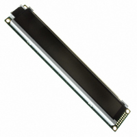
Manufacturer Part Number
C-51850NFJ-SLW-ADN
Description
LCD MOD CHAR 40X2 WHT TRANSFLECT
Manufacturer
Optrex America Inc
Series
C-51850r
Datasheets
1.C-51848NFJ-SLW-ADN.pdf
(2 pages)
2.C-51850NFJ-SLW-ADN.pdf
(1 pages)
3.C-51850NFJ-SLW-ADN.pdf
(17 pages)
Specifications of C-51850NFJ-SLW-ADN
Display Mode
Transflective
Display Type
STN - Super-Twisted Nematic
Number Of Digits/alpha
80
Outline L X W X H
116.00mm x 37.00mm x 15.60mm
Viewing Area
153.50mm L x 17.50mm W
Backlight
LED - White
Display Format
40 x 2
Character Size
5.85mm H x 3.20mm W
Character Format
5 x 8 Dots
Voltage - Supply
5.0V
Interface
Parallel
Operating Temperature
-20°C ~ 70°C
Character Count X Line
40 x 2
Module Size (w X H X T)
182 mm x 34.5 mm x 15.1 mm
Fluid Type
FSTN
Background Color
White
Backlight Type
LED White
Lead Free Status / RoHS Status
Lead free / RoHS Compliant
Dot Size
-
Lead Free Status / Rohs Status
Lead free / RoHS Compliant
Other names
73-1258


Recommended
Contrast Ratio
Viewing Angle
Response
C-51850NFJ-SLW-ADN (AD) No. 2005-0252
3. Optical Specifications
Note 1 : Voltage (Applied actual waveform to LCD Module) for the best contrast. The
Note 1 :Contrast ratio is definded as follows. (CR = L
Note 2 :The time that the luminance level reaches 90% of the saturation level from 0%
Note 3 :The time that the luminance level reaches 10% of the saturation level from
Note 4 :Definition of Driving Voltage V
3.1. LCD Driving Voltage
3.2. Optical Characteristics
LCD Driving Voltage
Time
Parameter
Parameter
when ON signal is applied.
100% when OFF signal is applied.
range of minimum and maximum shows tolerance of the operating voltage. The
specified contrast ratio and response time are not guaranteed over the entire range.
L
L
Measuring Spot : 3.0mm
V
Assuming that the typical driving waveforms shown below are applied to the LCD
Panel at 1/A Duty - 1/B Bias (A: Duty Number, B: Bias Number). Driving voltage
V
Vth1: The voltage V
Vth2: The voltage V
ON
OFF
OD
OD
Rise Note 2
Decay Note 3
V
=V
: Luminance of the OFF segments
is definded as follows.
: Luminance of the ON segments
OD
Vo-p
luminance at the segment which the ON signal is applied to.
luminance at the segment which the OFF signal is applied to.
CC
= (Vth1+Vth2) / 2
Note 1
-V
Note 1
ADJ
1/( f
( ON SIGNAL )
-V
F
BE
A )
O-P
O-P
V
Symbol
Symbol
CC
T
T
CR
OFF
that should provide 70% of the saturation level in the
that should provide 20% of the saturation level in the
ON
-V
EE
OD
Ta=25 C, 1/16 Duty, 1/4 Bias, V
Conditions
Conditions
= 0 C , =-
Ta= -20 C
Ta=25 C
Ta=70 C
-
-
ON
OPTREX CORPORATION
/ L
OFF
1 /f
)
( OFF SIGNAL )
Shown in 3.3
F
Min.
Min.
4.4
4.2
-
-
-
-
OD
=4.8V (Note 4), = 0 , =-
( B-2 ) Vo-p/B
Typ.
Typ.
130
4.8
5.0
80
-
-
Max.
Max.
160
200
5.2
5.2
-
-
Page 7/17
Units
Units
ms
ms
V
V
V
Related parts for C-51850NFJ-SLW-ADN
Image
Part Number
Description
Manufacturer
Datasheet
Request
R

Part Number:
Description:
LCD 6.5" TFT MOD 640X480 VGA
Manufacturer:
Optrex America Inc

Part Number:
Description:
LCD Graphic Display Modules & Accessories OPTREX
Manufacturer:
Optrex America Inc

Part Number:
Description:
LCD MODULE 16X2 CHARACTER
Manufacturer:
Optrex America Inc
Datasheet:

Part Number:
Description:
LCD MOD CHAR 20X2 TRANSMISSIVE
Manufacturer:
Optrex America Inc
Datasheet:

Part Number:
Description:
LCD MODULE 16X1 W/LED BACKLIGHT
Manufacturer:
Optrex America Inc
Datasheet:

Part Number:
Description:
LCD MOD CHAR 16X2 WHT TRANSFLECT
Manufacturer:
Optrex America Inc
Datasheet:

Part Number:
Description:
LCD MODULE 20X2 GREEN CHARACTER
Manufacturer:
Optrex America Inc
Datasheet:

Part Number:
Description:
LCD MODULE 20X2 BLUE CHARACTER
Manufacturer:
Optrex America Inc
Datasheet:

Part Number:
Description:
LCD MODULE 20X2 WHITE CHARACTER
Manufacturer:
Optrex America Inc
Datasheet:
Part Number:
Description:
LCD MOD 16X2 CHARAC TRANS W/LED
Manufacturer:
Optrex America Inc
Datasheet:

Part Number:
Description:
LCD MOD CHAR 20X4 WHT TRANSFLECT
Manufacturer:
Optrex America Inc
Datasheet:

Part Number:
Description:
LCD MODULE 16X2 HI CONT STD LED
Manufacturer:
Optrex America Inc

Part Number:
Description:
LCD MOD CHAR 20X4 WHT TRANSMISS
Manufacturer:
Optrex America Inc
Datasheet:

Part Number:
Description:
LCD MOD CHAR 16X2 WHT TRANSMISS
Manufacturer:
Optrex America Inc
Datasheet:

Part Number:
Description:
LCD MOD 16X2 CHARAC TRANS W/LED
Manufacturer:
Optrex America Inc
Datasheet: