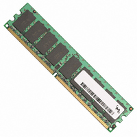
MT18HVF12872PY-667D1 Micron Technology Inc, MT18HVF12872PY-667D1 Datasheet - Page 9

MT18HVF12872PY-667D1
Manufacturer Part Number
MT18HVF12872PY-667D1
Description
MODULE DDR2 512MB 240-DIMM
Manufacturer
Micron Technology Inc
Specifications of MT18HVF12872PY-667D1
Memory Type
DDR2 SDRAM
Memory Size
1GB
Speed
667MT/s
Package / Case
240-DIMM
Main Category
DRAM Module
Sub-category
DDR2 SDRAM
Module Type
240RDIMM
Device Core Size
72b
Organization
128Mx72
Total Density
1GByte
Chip Density
512Mb
Access Time (max)
45ps
Maximum Clock Rate
667MHz
Operating Supply Voltage (typ)
1.8V
Operating Current
3.24A
Number Of Elements
18
Operating Supply Voltage (max)
1.9V
Operating Supply Voltage (min)
1.7V
Operating Temp Range
0C to 70C
Operating Temperature Classification
Commercial
Pin Count
240
Mounting
Socket
Lead Free Status / RoHS Status
Lead free / RoHS Compliant
Register and PLL Specifications
Table 9:
PDF: 09005aef82255aba/Source: 09005aef81c753af
HVF18C128x72.fm - Rev. C 3/07 EN
DC high-level
input voltage
DC low-level
input voltage
AC high-level
input voltage
AC low-level
input voltage
Common-mode input
voltage range
Differential input
voltage
Output high voltage
Output low voltage
Input current
Static standby
Static operating
Dynamic operating –
clock tree
Dynamic operating
(per each input)
Input capacitance
(per device, per pin)
Input capacitance
(per device, per pin)
Input capacitance
(per device, per pin)
Parameter
Register Specifications
SSTU32865 devices or equivalent JESD82-19
Notes:
Symbol
V
V
V
V
I
I
IH
IH
V
V
IL
IL
V
1. Timing and switching specifications for the register listed above are critical for proper oper-
V
I
I
DDD
DDD
DD
DD
C
C
C
ICR
OH
(
(
OL
I
(
(
ID
I
DC
AC
DC
AC
I
I
I
ation of the DDR2 SDRAM registered DIMMs. These are meant to be a subset of the param-
eters for the specific device used on the module. Detailed information for this register is
available in JEDEC Standard JESD82.
)
)
)
)
Parity output
Parity output
Data inputs
command
command
command
command
Address,
Address,
Address,
Address,
control,
control,
control,
control,
CK, CK#
CK, CK#
CK, CK#
All pins
All pins
All pins
RESET#
Pins
N/A
N/A
1GB (x72, ECC, SR) 240-Pin DDR2 SDRAM VLP RDIMM
RESET# = V
RESET# = V
One data input switching at
V
V
V
switching 50% duty cycle;
switching 50% duty cycle
ICR
IL
IL
RESET# = V
t
V
(
(
CK/2, 50% duty cycle
AC
AC
V
I
= 900mV, V
V
V
= V
I
I
RESET# = V
I
), I
), I
= V
= V
= V
V
9
Condition
V
IH
O
O
DD
LVCMOS
LVCMOS
SSTL_18
SSTL_18
SSTL_18
SSTL_18
SSTL_18
SSTL_18
DD
DD
DD
DD
REF
DD
(
I
= 0; CK and CK#
= 0; CK and CK#
AC
Q = 1.8V
O
, V
, V
= 1.8V
Q or V
Q or V
= 0
SS
) or V
±250mV;
I
I
Q (I
ID
= V
= V
SS
Micron Technology, Inc., reserves the right to change products or specifications without notice.
= 600mV;
O
Q;
IL
SS
IH
IH
SS
(
= 0)
Q
(
(
Q
DC
AC
AC
)
) or
) or
Register and PLL Specifications
V
V
REF
REF
(
(
Min
DC
DC
0.67
0.6
1.2
2.5
–5
0
–
–
–
–
–
–
2
–
) + 125
) + 250
©2003 Micron Technology, Inc. All rights reserved.
manufacturer
manufacturer
manufacturer
V
V
REF
REF
Varies by
Varies by
Varies by
1.125
(
(
Max
DC
DC
200
0.5
3.5
80
–
–
–
–
5
3
) - 125
) - 250
Units
mV
mV
mV
mV
mA
µA
µA
µA
µA
pF
pF
pF
V
V
V
V


