MT9HVF6472PY-667D1 Micron Technology Inc, MT9HVF6472PY-667D1 Datasheet
MT9HVF6472PY-667D1
Specifications of MT9HVF6472PY-667D1
MT9HVF6472PY-667D1


Related parts for MT9HVF6472PY-667D1


MT9HVF6472PY-667D1 Summary of contents
Page 1
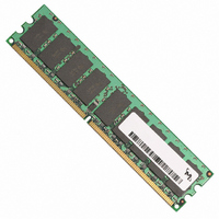
SR): 240-Pin DDR2 SDRAM VLP RDIMM DDR2 SDRAM VLP Registered DIMM MT9HVF3272(P) – 256MB MT9HVF6472(P) – 512MB MT9HVF12872(P) – 1GB For component data sheets, refer to Micron’s Web site: Features • 240-pin, registered dual in-line memory ...
Page 2
... Density MT9HVF6472(P)Y-80E__ 512MB MT9HVF6472(P)Y-800__ 512MB MT9HVF6472(P)Y-667__ 512MB MT9HVF6472(P)Y-53E__ 512MB MT9HVF6472(P)Y-40E__ 512MB Table 5: Part Numbers and Timing Parameters – 1GB Modules Base device: MT47H128M8, 1Gb DDR2 SDRAM Module 1 Part Number Density MT9HVF12872(P)Y-80E__ MT9HVF12872(P)Y-800__ MT9HVF12872(P)Y-667__ MT9HVF12872(P)Y-53E__ MT9HVF12872(P)Y-40E__ Notes: 1. All part numbers end with a two-place code (not shown), designating component and PCB revisions ...
Page 3
Pin Assignments and Descriptions Table 6: Pin Assignments 240-Pin DDR2 RDIMM Front Pin Symbol Pin Symbol Pin DQ19 61 REF DQ0 33 DQ24 63 4 DQ1 34 DQ25 64 ...
Page 4
SR): 240-Pin DDR2 SDRAM VLP RDIMM Table 7: Pin Descriptions Pin numbers may not correlate with symbols; refer to Table 6 on page 3 for more information Symbol Type Description A[15:0] Input Address inputs: Provide the ...
Page 5
SR): 240-Pin DDR2 SDRAM VLP RDIMM Table 7: Pin Descriptions (continued) Pin numbers may not correlate with symbols; refer to Table 6 on page 3 for more information Symbol Type Description V Supply Reference voltage: V ...
Page 6
SR): 240-Pin DDR2 SDRAM VLP RDIMM Functional Block Diagram Figure 2: Functional Block Diagram RS0# DQS0 DQS0# DM0/DQS9 NC/DQS9# DQ0 DQ1 DQ2 DQ3 DQ4 DQ5 DQ6 DQ7 DQS1 DQS1# DM1/DQS10 NC/DQS10# DQ8 DQ9 DQ10 DQ11 DQ12 ...
Page 7
... READs and by the memory controller during WRITEs. DQS is edge- aligned with data for READs and center-aligned with data for WRITEs. DDR2 SDRAM modules operate from a differential clock (CK and CK#); the crossing of CK going HIGH and CK# going LOW will be referred to as the positive edge of CK. ...
Page 8
... Simulations can then render a considerably more accurate result. JEDEC modules are now designed by using simula- tions to close timing budgets. AC Timing and Operating Conditions Recommended AC operating conditions are given in the DDR2 component data sheets. Component specifications are available on Micron’ ...
Page 9
SR): 240-Pin DDR2 SDRAM VLP RDIMM I Specifications DD Table 10: DDR2 I Specifications and Conditions – 256MB DD Values shown are for MT47H32M8 DDR2 SDRAM only and are computed from values specified in the 256Mb ...
Page 10
SR): 240-Pin DDR2 SDRAM VLP RDIMM Table 11: DDR2 I Specifications and Conditions – 512MB DD Values shown are for MT47H64M8 DDR2 SDRAM only and are computed from values specified in the 512Mb (64 Meg x ...
Page 11
SR): 240-Pin DDR2 SDRAM VLP RDIMM Table 12: DDR2 I Specifications and Conditions (Die Revision A) – 1GB DD Values shown are for MT47H128M8 DDR2 SDRAM only and are computed from values specified in the 1Gb ...
Page 12
SR): 240-Pin DDR2 SDRAM VLP RDIMM Table 13: DDR2 I Specifications and Conditions (Die Revision E) – 1GB DD Values shown for MT47H64M8 DDR2 SDRAM only and are computed from values specified in the 512Mb (64 ...
Page 13
SR): 240-Pin DDR2 SDRAM VLP RDIMM Register and PLL Specifications Table 14: Register Specifications SSTU32866 devices or equivalent Parameter Symbol high-level IH DC input voltage DC low-level ...
Page 14
SR): 240-Pin DDR2 SDRAM VLP RDIMM Table 15: PLL Specifications CU877 device or equivalent JESD82-8.01 Parameter Symbol DC high-level input V IH voltage DC low-level input V IL voltage V Input voltage (limits high-level ...
Page 15
SR): 240-Pin DDR2 SDRAM VLP RDIMM Serial Presence-Detect Table 17: Serial Presence-Detect EEPROM DC Operating Conditions Parameter/Condition Supply voltage Input high voltage: Logic 1; All inputs Input low voltage: Logic 0; All inputs Output low voltage: ...
Page 16
SR): 240-Pin DDR2 SDRAM VLP RDIMM Module Dimensions Figure 3: 240-Pin DDR2 VLP RDIMM 2.00 (0.079) R (4X) U1 2.50 (0.098) D (2X) 2.30 (0.091) TYP PIN 1 1.0 (0.039) 1.0 (0.039) TYP TYP U8 U9 ...