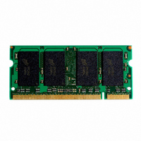
MT8LSDT3264HY-13ED2 Micron Technology Inc, MT8LSDT3264HY-13ED2 Datasheet

MT8LSDT3264HY-13ED2
Specifications of MT8LSDT3264HY-13ED2
MT8LSDT3264HY-13ED2
Related parts for MT8LSDT3264HY-13ED2
MT8LSDT3264HY-13ED2 Summary of contents
Page 1
... PRODUCTS AND SPECIFICATIONS DISCUSSED HEREIN ARE SUBJECT TO CHANGE BY MICRON WITHOUT NOTICE. 64MB, 128MB, 256MB (x64, DR) MT8LSDT864(L)H(I) – 64MB MT8LSDT1664(L)H(I) – 128MB MT8LSDT3264(L)H(I) – 256MB For the latest data sheet, please refer to the Micron site: www.micron.com/products/modules Figure 1: 144-Pin SODIMM (MO-190) Standard 1.25in. (31.75mm) Options • Self Refresh Current Standard Low-Power • ...
Page 2
Table 3: Part Numbers 1 PART NUMBER MT8LSDT864(L)HG-13E_ MT8LSDT864(L)HY-13E_ MT8LSDT864(L)H(I)G-133_ MT8LSDT864(L)H(I)Y-133_ MT8LSDT864(L)HG-10E_ MT8LSDT864(L)HY-10E_ MT8LSDT1664(L)HG-13E_ MT8LSDT1664(L)HY-13E_ MT8LSDT1664(L)H(I)G-133_ MT8LSDT1664(L)H(I)Y-133_ MT8LSDT1664(L)HG-10E_ MT8LSDT1664(L)HY-10E_ MT8LSDT3264(L)HG-13E_ MT8LSDT3264(L)HY-13E_ MT8LSDT3264(L)H(I)G-133_ MT8LSDT3264(L)H(I)Y-133_ MT8LSDT3264(L)HG-10E_ MT8LSDT3264(L)HY-10E_ NOTE: 1. The designators for component and PCB revision are the last two characters of ...
Page 3
... A2 69 S0# 105 S1# 107 SS NOTE: 1. Pin Connect for 64MB and128MB modules, or A12 for 256MB module. Figure 2: Pin Locations (144-Pin SODIMM) Front View U2 U3 PIN 1 (all odd pins) 09005aef8077d63a SD8C8_16_32x64HG.fm - Rev. C 6/04 EN 64MB, 128MB, 256MB (x64, DR) Table 5: PIN SYMBOL PIN SYMBOL PIN SYMBOL PIN SYMBOL ...
Page 4
... Not Connected: These pins should be left unconnected. DNU – Do Not Use: These pins are not connected on these modules, but are assigned pins on other modules in this product family. 4 144-PIN SDRAM SODIMM Micron Technology, Inc., reserves the right to change products or specifications without notice. ...
Page 5
... WE# A0-A11 (64MB/128MB) A0-A12 (256MB) BA0-1 NOTE: 1. All resistor values are 10 unless otherwise specified. 2. Per industry standard, Micron modules use various component speed grades as referenced in the module part numbering guide at: www.micron.com/support/numbering.html. 09005aef8077d63a SD8C8_16_32x64HG.fm - Rev. C 6/04 EN 64MB, 128MB, 256MB (x64, DR) Figure 3: Functional Block Diagram ...
Page 6
... An auto pre- charge function may be enabled to provide a self- timed row precharge that is initiated at the end of the burst sequence. These modules use an internal pipe- lined architecture to achieve high-speed operation. This architecture is compatible with the 2n rule of prefetch architectures, but it also allows the column address to be changed on every clock cycle to achieve a high-speed, fully random access ...
Page 7
Mode register bits M0–M2 specify the burst length, M3 specifies the type of burst (sequential or inter- leaved), M4–M6 specify the CAS latency, M7 and M8 specify the operating mode, M9 specifies the write burst mode, and M10 and M11 ...
Page 8
... For a burst length of one, A0–Ai select the unique col- umn to be accessed, and mode register bit M3 is ignored for 64MB modules for 128MB and 256MB modules 09005aef8077d63a SD8C8_16_32x64HG.fm - Rev. C 6/04 EN 64MB, 128MB, 256MB (x64, DR) Figure 5: CAS Latency Diagram ...
Page 9
Test modes and reserved states should not be used, because unknown operation or incompatibility with future versions may result. Write Burst Mode When the burst length programmed via M0- M2 applies to both READ and WRITE bursts; ...
Page 10
Commands The Truth Table provides a quick reference of avail- able commands. This is followed by written descrip- tion of each command. For a more detailed des- Table 9: Truth Table – SDRAM Commands and DQMB Operation CKE is HIGH ...
Page 11
Absolute Maximum Ratings Stresses greater than those listed may cause perma- nent damage to the device. This is a stress rating only, and functional operation of the device at these or any other conditions above those indicated in the opera- ...
Page 12
Table 12: I Specifications and Conditions – 128MB DD Notes 11, 13; notes appear on page 15; V PARAMETER/CONDITION OPERATING CURRENT: Active Mode; Burst = 2; READ or WRITE (MIN) STANDBY CURRENT: Power-Down ...
Page 13
Table 14: Capacitance Notes 1, 2; notes appear on page 15 PARAMETER Input Capacitance: Address and Command Input Capacitance: CK, CKE, S# Input Capacitance: DQMB Inuput/Output Capacitnance: DQ Table 15: Electrical Characteristics and Recommended AC Operating Conditions Notes ...
Page 14
Table 16: AC Functional Characteristics Notes 11, 31; notes appear on page 15 PARAMETER READ/WRITE command to READ/WRITE command CKE to clock disable or power-down entry mode CKE to clock enable or power-down exit setup ...
Page 15
Notes 1. All voltages referenced This parameter is sampled MHz 25°C; pin under test biased at A 1.4V dependent on output loading and cycle DD rates. Specified ...
Page 16
SPD Clock and Data Conventions Data states on the SDA line can change only during SCL LOW. SDA state changes during SCL HIGH are reserved for indicating start and stop conditions (Fig- ure 6, Data Validity, and Figure 7, Definition ...
Page 17
Table 17: EEPROM Device Select code The most significant bit (b7) is sent first Memory Area Select Code (two arrays) Protection Register Select Code Table 18: EEPROM Operating modes MODE RW BIT Current Address Read Random Address Read Sequential Read ...
Page 18
Table 19: Serial Presence-Detect EEPROM DC Operating Conditions All voltages referenced DDSPD PARAMETER/CONDITION SUPPLY VOLTAGE INPUT HIGH VOLTAGE: Logic 1; All inputs INPUT LOW VOLTAGE: Logic 0; All inputs OUTPUT LOW VOLTAGE 3mA ...
Page 19
Table 21: Serial Presence-Detect Matrix “1”/”0”: Serial Data, “driven to HIGH”/”driven to LOW”; notes appear at end of Serial Presence-Detect Matrix BYTE DESCRIPTION 0 Number of Bytes Used by Micron 1 Total Number of SPD Memory Bytes 2 Memory Type ...
Page 20
... Week of Manufacture in BCD 95-98 Module Serial Number 99-125 Manufacturer-specific Data (RSVD) 126 System Frequency 127 SDRAM Component & Clock Detail NOTE The value of RAS used for -13E modules is calculated from 09005aef8077d63a SD8C8_16_32x64HG.fm - Rev. C 6/04 EN 64MB, 128MB, 256MB (x64, DR) ENTRY (VERSION) 32MB, 64MB, or 128MB ...
Page 21
R (2X) U2 0.071 (1.80) (2X) 0.236 (6.00) 0.100 (2.55) 0.079 (2.00) PIN 1 0.13 (3.30) U9 PIN 144 NOTE: All dimensions in inches (millimeters); Data Sheet Designation Released (No Mark): This data sheet contains mini- mum and ...


