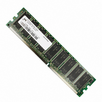
MT9VDDT6472AG-335D1 Micron Technology Inc, MT9VDDT6472AG-335D1 Datasheet - Page 9

MT9VDDT6472AG-335D1
Manufacturer Part Number
MT9VDDT6472AG-335D1
Description
MODULE DDR SDRAM 512MB 184-DIMM
Manufacturer
Micron Technology Inc
Datasheet
1.MT9VDDT6472AG-335D1.pdf
(27 pages)
Specifications of MT9VDDT6472AG-335D1
Memory Type
DDR SDRAM
Memory Size
512MB
Speed
167MHz
Package / Case
184-DIMM
Lead Free Status / RoHS Status
Contains lead / RoHS non-compliant
Other names
557-1137
Table 6:
NOTE:
Table 7:
pdf: 09005aef80a43e7d, source: 09005aef80a43d77
DDA9C16_32_64x72AG.fm - Rev. B 9/04 EN
1. For a burst length of two, A1
2. or a burst length of four, A2
3. For a burst length of eight, A3
4. Whenever a boundary of the block is reached within a
5. i = 9 (128MB, 256MB)
LENGTH
BURST
element block; A0 selects the first access within the
block.
ment block; A0
block.
element block; A0
block.
given sequence above, the following access wraps
within the block.
i = 9, 11 (512MB)
SPEED
2
4
8
-40B
A2 A1 A0
STARTING
ADDRESS
0
0
0
0
1
1
1
1
COLUMN
A1 A0
Burst Definition Table
CAS Latency (CL) Table
0
0
1
1
0
0
1
1
0
0
1
1
75
–
A1 select the first access within the
CL = 2
A0
0
1
0
1
0
1
0
1
0
1
0
1
0
1
–
f
A2 select the first access within the
ALLOWABLE OPERATING
0-1-2-3-4-5-6-7
1-2-3-4-5-6-7-0
2-3-4-5-6-7-0-1
3-4-5-6-7-0-1-2
4-5-6-7-0-1-2-3
5-6-7-0-1-2-3-4
6-7-0-1-2-3-4-5
7-0-1-2-3-4-5-6
ORDER OF ACCESSES WITHIN A
SEQUENTIAL
133
FREQUENCY (MHZ)
TYPE =
0-1-2-3
1-2-3-0
2-3-0-1
3-0-1-2
0-1
1-0
–
75
–
Ai select the four-data-ele-
CL = 2.5
Ai select the two-data-
–
Ai select the eight-data-
f
BURST
167 125
0-.1-2-3-4-5-6-7
128MB, 256MB, 512MB (x72, ECC, SR), PC3200
INTERLEAVED
1-0-3-2-5-4-7-6
2-3-0-1-6-7-4-5
3-2-1-0-7-6-5-4
4-5-6-7-0-1-2-3
5-4-7-6-1-0-3-2
6-7-4-5-2-3-0-1
7-6-5-4-3-2-1-0
TYPE =
0-1-2-3
1-0-3-2
2-3-0-1
3-2-1-0
0-1
1-0
CL = 3
f
200
9
specifications recommend when a LOAD MODE REG-
ISTER command is issued to reset the DLL, it should
always be followed by a LOAD MODE REGISTER com-
mand to select normal operating mode.
(128MB), or A7–A12 (256MB, 512MB) are reserved for
future use and/or test modes.
reserved states should not be used because unknown
operation or incompatibility with future versions may
result.
Extended Mode Register
beyond those controlled by the mode register; these
additional functions are DLL enable/disable and out-
put drive strength. These functions are controlled via
the bits shown in Figure 6, Extended Mode Register
Definition Diagram, on page 10. The extended mode
register is programmed via the LOAD MODE REGIS-
TER command to the mode register (with BA0 = 1 and
COMMAND
COMMAND
COMMAND
Although not required by the Micron device, JEDEC
All other combinations of values for A7–A11
The extended mode register controls functions
DQS
DQS
DQS
CK#
CK#
CK#
DQ
DQ
DQ
Micron Technology, Inc., reserves the right to change products or specifications without notice.
Figure 5: CAS Latency Diagram
CK
CK
CK
184-Pin DDR SDRAM UDIMM
READ
READ
READ
Burst Length = 4 in the cases shown
Shown with nominal t AC, t DQSCK, and t DQSQ
T0
T0
T0
TRANSITIONING DATA
CL = 2
CL = 2.5
NOP
NOP
NOP
T1
T1
T1
CL = 3
T2
NOP
NOP
NOP
T2
T2
Test modes and
©2004 Micron Technology, Inc.
T2n
T2n
T2n
DON’T CARE
T3
NOP
NOP
NOP
T3
T3
T3n
T3n
T3n


