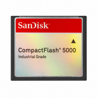
SDCFCR-001G-388 SanDisk, SDCFCR-001G-388 Datasheet - Page 46

SDCFCR-001G-388
Manufacturer Part Number
SDCFCR-001G-388
Description
COMPACT FLASH IND 1GB
Manufacturer
SanDisk
Datasheet
1.SDCFCF-001G-388.pdf
(97 pages)
Specifications of SDCFCR-001G-388
Memory Size
1GB
Memory Type
CompactFLASH
Lead Free Status / RoHS Status
Lead free / RoHS Compliant
- Current page: 46 of 97
- Download datasheet (3Mb)
SanDisk Industrial Grade CompactFlash 5000
4.4
When a CompactFlash Memory Card is configured in True IDE Mode the I/O
decoding is as listed in Table 34.
4.5
In accordance with the PCMCIA specification, each of the following registers
that is located at an odd offset address may be accessed at its normal address
and also the corresponding even address (normal address -1) using data bus
lines (D15-D8) when -CE1 is high and -CE2 is low, unless -IOIS16 is high (not
asserted) and an I/O cycle is being performed.
4.5.1
The Data Register is a 16-bit register and is used to transfer data blocks
between the CompactFlash Memory Card data buffer and the host. This
register overlaps the Error Register. The information in the following table
describes the combinations of data register access and is provided to assist in
understanding the overlapped Data Register and Error/Feature Register rather
than attempt to define general PCMCIA word and byte access modes and
operations. Refer to the PCMCIA PC Card Standard Release 2.0 for definitions
of the Card Accessing modes for I/O and memory cycles.
© 2007 SanDisk® Corporation
perform memory to memory block moves to the data register when the register
lies in memory space. Some hosts, such as the X86 processors, must increment
both the source and destination addresses when executing the memory to
memory block move instruction. Some PCMCIA socket adapters also have auto-
incrementing address logic embedded within them. This address window allows
these hosts and adapters to function efficiently. Note that this entire window
accesses the Data Register FIFO and does not allow random access to the data
buffer within the card.
1
1
1
1
1
1
1
1
0
0
True IDE Mode Addressing
ATA Registers
-CE2
Data Register (Address–1F0[170]; Offset 0, 8, 9)
0
0
0
0
0
0
0
0
1
1
-CE1
0
0
0
0
1
1
1
1
1
1
A2
Table 34: True IDE Mode I/O Decoding
0
0
1
1
0
0
1
1
1
1
A1
0
1
0
1
0
1
0
1
0
1
A0
39
Even RD Data
Error Register
Sector Count
Sector No.
Cylinder Low
Cylinder High
Select Card/Head
Status
Alt Status
Drive Address
-IORD=0
Even WR Data
Features
Sector Count
Sector No.
Cylinder Low
Cylinder High
Select Card/Head
Command
Device Control
Reserved
-IOWR=0
Product Manual
July 2007
Related parts for SDCFCR-001G-388
Image
Part Number
Description
Manufacturer
Datasheet
Request
R

Part Number:
Description:
COMPACT FLASH IND 512MB
Manufacturer:
SanDisk
Datasheet:

Part Number:
Description:
COMPACT FLASH IND 2GB
Manufacturer:
SanDisk
Datasheet:

Part Number:
Description:
COMPACT FLASH IND 4GB
Manufacturer:
SanDisk
Datasheet:

Part Number:
Description:
COMPACT FLASH IND 8GB
Manufacturer:
SanDisk
Datasheet:

Part Number:
Description:
IC MDOC G4 2GB 69-FBGA
Manufacturer:
SanDisk
Datasheet:

Part Number:
Description:
IC MDOC P3 256MB 48-TSOP
Manufacturer:
SanDisk
Datasheet:

Part Number:
Description:
IC MDOC P3 256MB 48-TSOP
Manufacturer:
SanDisk
Datasheet:

Part Number:
Description:
IC MDOC P3 256MB 48-TSOP
Manufacturer:
SanDisk
Datasheet:

Part Number:
Description:
IC MDOC H1 8GB 115-FBGA
Manufacturer:
SanDisk
Datasheet:

Part Number:
Description:
IC MDOC H3 1GB FBGA
Manufacturer:
SanDisk
Datasheet:


