VO4156D Vishay, VO4156D Datasheet - Page 3
VO4156D
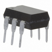
Manufacturer Part Number
VO4156D
Description
PHOTOTRIAC ZC 600V 1.6MA 6DIP
Manufacturer
Vishay
Datasheet
1.VO4154M.pdf
(6 pages)
Specifications of VO4156D
Isolation Voltage
5300 Vrms
Voltage - Isolation
5300Vrms
Number Of Channels
1
Voltage - Off State
600V
Output Type
AC, Triac, Zero Cross
Current - Gate Trigger (igt) (max)
1.6mA
Current - Hold (ih)
500µA
Current - Dc Forward (if)
60mA
Current - Output / Channel
300mA
Mounting Type
Through Hole
Package / Case
6-DIP (0.300", 7.62mm)
Configuration
1
Maximum Continuous Output Current
300 mA
Maximum Input Current
60 mA
Maximum Operating Temperature
+ 100 C
Maximum Power Dissipation
600 mW
Maximum Reverse Diode Voltage
6 V
Minimum Operating Temperature
- 55 C
Typical Input Voltage
1.2 V
Zero-crossing Circuit
Yes
Zero-crossing Voltage
20 V
Output Device
Triac
Peak Output Voltage (vdrm)
600 V
Maximum Input Voltage
1.4 V
Maximum Output Voltage
420 VAC
Minimum Trigger Current
1.6 mA (Max)
No. Of Channels
1
Optocoupler Output Type
Phototriac
Input Current
10mA
Output Voltage
600V
Opto Case Style
DIP
No. Of Pins
6
Input Current Max
10mA
Forward Voltage
1.2V
Rohs Compliant
Yes
Lead Free Status / RoHS Status
Lead free / RoHS Compliant


Note
• The thermal characteristics table above were measured at 25 °C and the thermal model is represented in the thermal network below. Each
Note
• Minimum and maximum values were tested requierements. Typical values are characteristics of the device and are the result of engineering
Document Number: 84797
Rev. 1.5, 20-Oct-10
THERMAL CHARACTERISTICS
PARAMETER
LED power dissipation
Output power dissipation
Maximum LED junction temperature
Maximum output die junction temperature
Thermal resistance, junction emitter to board
Thermal resistance, junction emitter to case
Thermal resistance, junction detector to board
Thermal resistance, junction detector to case
Thermal resistance, junction emitter to
junction detector
Thermal resistance, case to ambient
ELECTRICAL CHARACTERISTICS (T
PARAMETER
INPUT
Forward voltage
Reverse current
Input capacitance
OUTPUT
Repetitive peak off-state voltage
Off-state current
On-state voltage
On-state current
Off-state current in inhibit state
Holding current
Zero cross inhibit voltage
Critical rate of rise of off-state
voltage
Critical rate of rise of on-state
COUPLER
LED trigger current,
current required to latch output
Common mode coupling
capacitance
Capacitance (input to output)
resistance value given in this model can be used to calculate the temperatures at each node for a given operating condition. The thermal
resistance from board to ambient will be dependent on the type of PCB, layout and thickness of copper traces. For a detailed explanation
of the thermal model, please reference Vishay's Thermal Characteristics of Optocouplers application note.
evaluations. Typical values are for information only and are not part of the testing requirements.
Crossing, High dV/dt, Low Input Current
For technical questions, contact:
Optocoupler, Phototriac Output, Zero
V
D
PF = 1, V
= 0.67 V
f = 1 MHz, V
TEST CONDITION
V
V
F
D
I
F
I
= 0 V, f = 1 MHz
DRM
= V
I
I
= 2 mA, V
F
T
I
F
V
V
= rated I
= 300 mA
= 10 mA
SYMBOL
DRM,
R
D
amb
= 100 μA
T(RMS)
DRM
= 6 V
= 3 V
T
T
P
P
jmax.
jmax.
JDC
JEB
JEC
JDB
JED
diss
diss
CA
, T
I
= 25 °C, unless otherwise specified)
IO
F
DRM
= 0 A
= 1.7 V
FT
J
= 0 V
= 25 °C
VALUE
3563
100
500
125
125
150
139
103
496
78
optocoupleranswers@vishay.com
VO4154D/H/M
VO4156D/H/M
VO4154M
VO4156M
VO4154D
VO4154H
VO4156D
VO4156H
PART
UNIT
°C/W
°C/W
°C/W
°C/W
°C/W
°C/W
mW
mW
°C
°C
SYMBOL
dV/dt
dV/dt
V
V
I
I
C
V
DRM
DINH
C
I
V
I
I
I
I
I
I
V
DRM
DRM
C
TM
I
I
FT
FT
FT
FT
FT
FT
TM
CM
R
H
IH
IO
F
I
cr
cr
Vishay Semiconductors
T
19996
JD
MIN.
5000
400
600
8
θ
DB
VO4154, VO4156
θ
DC
T
T
TYP.
T
0.01
B
C
1.2
0.1
0.8
A
θ
25
DE
T
θ
θ
A
CA
BA
Package
θ
MAX.
EC
100
300
200
500
θ
1.4
1.6
1.6
10
20
www.vishay.com
EB
3
2
3
2
3
T
JE
UNIT
V/μs
A/μs
mA
mA
mA
mA
mA
mA
mA
μA
μA
μA
μA
pF
pF
pF
V
V
V
V
V
3
Related parts for VO4156D
Image
Part Number
Description
Manufacturer
Datasheet
Request
R

Part Number:
Description:
357-036-542-201 CARDEDGE 36POS DL .156 BLK LOPRO
Manufacturer:
Vishay
Datasheet:
Part Number:
Description:
357-036-542-201 CARDEDGE 36POS DL .156 BLK LOPRO
Manufacturer:
Vishay
Datasheet:
Part Number:
Description:
357-036-542-201 CARDEDGE 36POS DL .156 BLK LOPRO
Manufacturer:
Vishay
Datasheet:
Part Number:
Description:
357-036-542-201 CARDEDGE 36POS DL .156 BLK LOPRO
Manufacturer:
Vishay
Datasheet:
Part Number:
Description:
357-036-542-201 CARDEDGE 36POS DL .156 BLK LOPRO
Manufacturer:
Vishay
Datasheet:
Part Number:
Description:
357-036-542-201 CARDEDGE 36POS DL .156 BLK LOPRO
Manufacturer:
Vishay
Datasheet:
Part Number:
Description:
357-036-542-201 CARDEDGE 36POS DL .156 BLK LOPRO
Manufacturer:
Vishay
Datasheet:
Part Number:
Description:
357-036-542-201 CARDEDGE 36POS DL .156 BLK LOPRO
Manufacturer:
Vishay
Datasheet:
Part Number:
Description:
357-036-542-201 CARDEDGE 36POS DL .156 BLK LOPRO
Manufacturer:
Vishay
Datasheet:
Part Number:
Description:
357-036-542-201 CARDEDGE 36POS DL .156 BLK LOPRO
Manufacturer:
Vishay
Datasheet:
Part Number:
Description:
357-036-542-201 CARDEDGE 36POS DL .156 BLK LOPRO
Manufacturer:
Vishay
Datasheet:
Part Number:
Description:
357-036-542-201 CARDEDGE 36POS DL .156 BLK LOPRO
Manufacturer:
Vishay
Datasheet:
Part Number:
Description:
357-036-542-201 CARDEDGE 36POS DL .156 BLK LOPRO
Manufacturer:
Vishay
Datasheet:
Part Number:
Description:
357-036-542-201 CARDEDGE 36POS DL .156 BLK LOPRO
Manufacturer:
Vishay
Datasheet:
Part Number:
Description:
357-036-542-201 CARDEDGE 36POS DL .156 BLK LOPRO
Manufacturer:
Vishay
Datasheet: