VO3063 Vishay, VO3063 Datasheet - Page 2
VO3063
Manufacturer Part Number
VO3063
Description
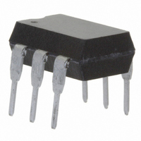
PHOTOTRIAC ZC 600V 5MA 6DIP
Manufacturer
Vishay
Specifications of VO3063
No. Of Channels
1
Input Current
30mA
Output Voltage
600V
Opto Case Style
DIP
No. Of Pins
6
Isolation Voltage
5.3kV
Voltage - Isolation
5300Vrms
Number Of Channels
1
Voltage - Off State
600V
Output Type
AC, Triac, Zero Cross
Current - Gate Trigger (igt) (max)
5mA
Current - Hold (ih)
200µA
Current - Dc Forward (if)
60mA
Current - Output / Channel
100mA
Mounting Type
Through Hole
Package / Case
6-DIP (0.300", 7.62mm)
Optocoupler Output Type
Phototriac
Input Current Max
30mA
Number Of Elements
1
Output Device
Triac
Forward Voltage
1.5V
Repetitive Peak Off-state Volt
600V
Operating Temp Range
-40C to 100C
Output Current
100mA
Package Type
PDIP
Reverse Breakdown Voltage
6V
Mounting
Through Hole
Pin Count
6
Trigger Current
5mA
Zero Crossing Circuit
Yes
Operating Temperature Classification
Industrial
Forward Current
60mA
Power Dissipation
300mW
Rohs Compliant
Yes
Lead Free Status / RoHS Status
Lead free / RoHS Compliant
Lead Free Status / RoHS Status
Lead free / RoHS Compliant, Lead free / RoHS Compliant
Other names
751-1383-5
VO3063
VO3063
Available stocks
Company
Part Number
Manufacturer
Quantity
Price

Part Number:
VO3063-X017T
Manufacturer:
VISHAY/威世
Quantity:
20 000


VO3062, VO3063
Vishay Semiconductors
Notes
(1)
(2)
Note
The thermal model is represented in the thermal network below. Each resistance value given in this model can be used to calculate the
temperatures at each node for a given operating condition. The thermal resistance from board to ambient will be dependent on the type of PCB,
layout and thickness of copper traces. For a detailed explanation of the thermal model, please reference Vishay’s Thermal Characteristics of
Optocouplers application note.
www.vishay.com
928
ABSOLUTE MAXIMUM RATINGS
PARAMETER
COUPLER
Isolation test voltage
Total power dissipation
Operating temperature range
Storage temperature range
Soldering temperature
THERMAL CHARACTERISTICS
PARAMETER
Maximum LED junction temperature
Maximum output die junction temperature
Thermal resistance, junction emitter to board
Thermal resistance, junction emitter to case
Thermal resistance, junction detector to board
Thermal resistance, junction detector to case
Thermal resistance, junction emitter to
junction detector
Thermal resistance, case to ambient
ELECTRICAL CHARACTERISTCS
PARAMETER
INPUT
Reverse current
Forward voltage
OUTPUT
Leakage with LED off, either direction
Critical rate of rise off-state voltage
T
Stresses in excess of the absolute maximum ratings can cause permanent damage to the device. Functional operation of the device is not
implied at these or any other conditions in excess of those given in the operational sections of this document. Exposure to absolute maximum
ratings for extended periods of the time can adversely affect reliability.
Refer to reflow profile for soldering conditions for surface mounted devices (SMD). Refer to wave profile for soldering conditions for through
hole devices (DIP).
amb
= 25 °C, unless otherwise specified.
(2)
For technical questions, contact:
TEST CONDITION
TEST CONDITION
V
maximum ≤ 10 s
V
I
DRM
SYMBOL
F
V
D
(1)
= 30 mA
R
T
T
θ
θ
θ
θ
θ
= 400 V
θ
jmax.
jmax.
t = 1 s
JEB
JEC
JDB
JDC
JED
= 6 V
= 600 V
CA
Phototriac, Zero Crossing,
1.5 kV/µs dV/dt, 600 V
VALUE
3563
125
125
150
139
103
496
78
optocoupleranswers@vishay.com
PART
PART
°C/W
°C/W
°C/W
°C/W
°C/W
°C/W
UNIT
°C
°C
SYMBOL
dV/dt
I
DRM
V
I
R
F
SYMBOL
V
T
P
T
T
amb
ISO
stg
sld
tot
T
1500
19996
MIN.
JD
θ
DB
θ
DC
- 40 to + 100
- 55 to + 150
TYP.
2000
T
T
T
VALUE
B
1.2
C
A
θ
10
5300
DE
Document Number: 83748
300
260
T
θ
θ
A
CA
BA
Package
Rev. 1.8, 03-Sep-09
θ
EC
MAX.
θ
EB
500
1.5
10
T
JE
UNIT
V
mW
°C
°C
°C
RMS
UNIT
V/µs
µA
nA
V
Related parts for VO3063
Image
Part Number
Description
Manufacturer
Datasheet
Request
R

Part Number:
Description:
357-036-542-201 CARDEDGE 36POS DL .156 BLK LOPRO
Manufacturer:
Vishay
Datasheet:
Part Number:
Description:
357-036-542-201 CARDEDGE 36POS DL .156 BLK LOPRO
Manufacturer:
Vishay
Datasheet:
Part Number:
Description:
357-036-542-201 CARDEDGE 36POS DL .156 BLK LOPRO
Manufacturer:
Vishay
Datasheet:
Part Number:
Description:
357-036-542-201 CARDEDGE 36POS DL .156 BLK LOPRO
Manufacturer:
Vishay
Datasheet:
Part Number:
Description:
357-036-542-201 CARDEDGE 36POS DL .156 BLK LOPRO
Manufacturer:
Vishay
Datasheet:
Part Number:
Description:
357-036-542-201 CARDEDGE 36POS DL .156 BLK LOPRO
Manufacturer:
Vishay
Datasheet:
Part Number:
Description:
357-036-542-201 CARDEDGE 36POS DL .156 BLK LOPRO
Manufacturer:
Vishay
Datasheet:
Part Number:
Description:
357-036-542-201 CARDEDGE 36POS DL .156 BLK LOPRO
Manufacturer:
Vishay
Datasheet:
Part Number:
Description:
357-036-542-201 CARDEDGE 36POS DL .156 BLK LOPRO
Manufacturer:
Vishay
Datasheet:
Part Number:
Description:
357-036-542-201 CARDEDGE 36POS DL .156 BLK LOPRO
Manufacturer:
Vishay
Datasheet:
Part Number:
Description:
357-036-542-201 CARDEDGE 36POS DL .156 BLK LOPRO
Manufacturer:
Vishay
Datasheet:
Part Number:
Description:
357-036-542-201 CARDEDGE 36POS DL .156 BLK LOPRO
Manufacturer:
Vishay
Datasheet:
Part Number:
Description:
357-036-542-201 CARDEDGE 36POS DL .156 BLK LOPRO
Manufacturer:
Vishay
Datasheet:
Part Number:
Description:
357-036-542-201 CARDEDGE 36POS DL .156 BLK LOPRO
Manufacturer:
Vishay
Datasheet:
Part Number:
Description:
357-036-542-201 CARDEDGE 36POS DL .156 BLK LOPRO
Manufacturer:
Vishay
Datasheet: