TLP181(GB-TPR,F,T) Toshiba, TLP181(GB-TPR,F,T) Datasheet - Page 5
TLP181(GB-TPR,F,T)
Manufacturer Part Number
TLP181(GB-TPR,F,T)
Description
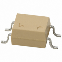
PHOTOCOUPLER TRANS OUT 4-SMD
Manufacturer
Toshiba
Specifications of TLP181(GB-TPR,F,T)
Number Of Channels
1
Input Type
DC
Voltage - Isolation
3750Vrms
Current Transfer Ratio (min)
100% @ 5mA
Current Transfer Ratio (max)
600% @ 5mA
Voltage - Output
80V
Current - Output / Channel
50mA
Current - Dc Forward (if)
50mA
Vce Saturation (max)
400mV
Output Type
Transistor
Mounting Type
Surface Mount
Package / Case
4-SMD
Output Device
Transistor
Number Of Elements
1
Reverse Breakdown Voltage
5V
Forward Voltage
1.3V
Forward Current
50mA
Collector-emitter Voltage
80V
Package Type
MFSOP
Collector Current (dc) (max)
50mA
Isolation Voltage
3750Vrms
Power Dissipation
200mW
Collector-emitter Saturation Voltage
0.4V
Current Transfer Ratio
600%
Pin Count
4
Mounting
Surface Mount
Operating Temp Range
-25C to 85C
Operating Temperature Classification
Commercial
Maximum Collector Emitter Voltage
80 V
Maximum Collector Emitter Saturation Voltage
0.4 V
Maximum Forward Diode Voltage
1.3 V
Maximum Collector Current
10 mA
Maximum Power Dissipation
200 mW
Maximum Operating Temperature
+ 100 C
Minimum Operating Temperature
- 55 C
Maximum Fall Time
3 us
Maximum Input Diode Current
50 mA
Maximum Reverse Diode Voltage
5 V
Maximum Rise Time
2 us
Lead Free Status / RoHS Status
Lead free / RoHS Compliant
Other names
TLP181(GB-TPR)
TLP181GBFTR
TLP181GBTPR
TLP181GBTPRFT
TLP181GBTR
TLP181GBTR
TLP181GBFTR
TLP181GBTPR
TLP181GBTPRFT
TLP181GBTR
TLP181GBTR


Switching Characteristics
Rise time
Fall time
Turn−on time
Turn−off time
Turn−on time
Storage time
Turn−off time
I
F
Fig. 1
Switching time test circuit
Characteristic
(Ta = 25°C)
R
L
Symbol
V
V
t
CC
t
OFF
CE
t
t
ON
on
off
t
t
t
s
r
f
V
R
R
V
CC
CC
L
L
= 100Ω
= 1.9 kΩ
5
= 10 V, I
= 5 V, I
Test Condition
I
V
F
F
t
CE
ON
C
= 16 mA
= 2 mA
t
S
(Fig.1)
t
OFF
Min
—
—
—
—
—
—
—
4.5V
0.5V
Typ.
25
40
2
3
3
3
2
2009-11-12
Max
—
—
—
—
—
—
—
TLP181
Unit
μs
μs
Related parts for TLP181(GB-TPR,F,T)
Image
Part Number
Description
Manufacturer
Datasheet
Request
R

Part Number:
Description:
PHOTOCOUPLER TRANS OUT 6MFSOP-4
Manufacturer:
Toshiba
Datasheet:

Part Number:
Description:
PHOTOCOUPLER TRANS-OUT 4-SMD
Manufacturer:
Toshiba
Datasheet:
Part Number:
Description:
Transistor Output Optocouplers 80Vceo 3750Vrms High CTR
Manufacturer:
Toshiba
Part Number:
Description:
PHOTOCOUPLER TRANS-OUT 4-SMD
Manufacturer:
Toshiba
Datasheet:
Part Number:
Description:
IC OPTOCOUPL AC/DC-IN 1-CH TRANS DC-OUT 4MFSOP
Manufacturer:
Toshiba
Datasheet:
Part Number:
Description:
GaAs IRED & PHOTO-TRANSISTOR
Manufacturer:
Toshiba
Datasheet:

Part Number:
Description:
Toshiba Semiconductor [TOSHIBA IGBT Module Silicon N Channel IGBT]
Manufacturer:
TOSHIBA Semiconductor CORPORATION
Datasheet:
Part Number:
Description:
TOSHIBA GTR MODULE SILICON NPN TRIPLE DIFFUSED TYPE
Manufacturer:
TOSHIBA Semiconductor CORPORATION
Datasheet:
Part Number:
Description:
TOSHIBA GTR Module Silicon N Channel IGBT
Manufacturer:
TOSHIBA Semiconductor CORPORATION
Datasheet:
Part Number:
Description:
TOSHIBA Intelligent Power Module Silicon N Channel IGBT
Manufacturer:
TOSHIBA Semiconductor CORPORATION
Datasheet:
Part Number:
Description:
TOSHIBA INTELLIGENT POWER MODULE SILICON N CHANNEL LGBT
Manufacturer:
TOSHIBA Semiconductor CORPORATION
Datasheet:
Part Number:
Description:
TOSHIBA IGBT Module Silicon N Channel IGBT
Manufacturer:
TOSHIBA Semiconductor CORPORATION
Datasheet:
Part Number:
Description:
TOSHIBA GTR MODULE SILICON N−CHANNEL IGBT
Manufacturer:
TOSHIBA Semiconductor CORPORATION
Datasheet:
Part Number:
Description:
TOSHIBA Intelligent Power Module Silicon N Channel IGBT
Manufacturer:
TOSHIBA Semiconductor CORPORATION
Datasheet: