4N46-000E Avago Technologies US Inc., 4N46-000E Datasheet - Page 7
4N46-000E
Manufacturer Part Number
4N46-000E
Description
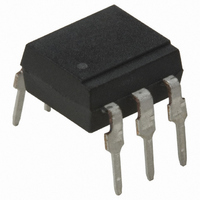
OPTOCOUPLER DARL-OUT 6-DIP
Manufacturer
Avago Technologies US Inc.
Type
Analogr
Datasheet
1.4N46.pdf
(11 pages)
Specifications of 4N46-000E
Input Type
DC
Package / Case
6-DIP (0.300", 7.62mm)
Number Of Channels
1
Voltage - Isolation
3750Vrms
Current Transfer Ratio (min)
200% @ 10mA
Current Transfer Ratio (max)
1000% @ 10mA
Voltage - Output
4.5V
Current - Output / Channel
60mA
Current - Dc Forward (if)
10mA
Output Type
Darlington with Base
Mounting Type
Through Hole
Isolation Voltage
3750 Vrms
Maximum Continuous Output Current
60 mA
Maximum Forward Diode Current
20 mA
Output Device
Darlington With Base
Configuration
1 Channel
Current Transfer Ratio
3200 %
Maximum Baud Rate
100 KBps
Maximum Forward Diode Voltage
1.7 V
Maximum Reverse Diode Voltage
5 V
Maximum Input Diode Current
20 mA
Maximum Power Dissipation
100 mW
Maximum Operating Temperature
+ 70 C
Minimum Operating Temperature
0 C
Package Type
6-Pin DIP
Lead Free Status / RoHS Status
Lead free / RoHS Compliant
Vce Saturation (max)
-
Lead Free Status / Rohs Status
Lead free / RoHS Compliant
Other names
516-1596-5
Available stocks
Company
Part Number
Manufacturer
Quantity
Price
Company:

Part Number:
4N46-000E
Manufacturer:
AVG
Quantity:
452
Part Number:
4N46-000E
Manufacturer:
AVAGO/安华高
Quantity:
20 000


Recommended Operating Conditions
7
DC Electrical Specifications
Over recommended temperature (T
Switching Specifications
(Over recommended temperature T
*JEDEC Registered Data.
**All typicals at T
Parameter
Propagation Delay Time
to Logic Low at Output
Propagation Delay Time
to Logic High at Output
Common Mode
Transient Immunity at
High Output Level
Common Mode
Transient Immunity at
Low Output Level
Parameter
Output Voltage (4N46)
Output Voltage (4N45)
Input Current (High)
Input Voltage (Low)
Operating Temperature
Output Current
Parameter
Current Transfer
Ratio
Logic Low
Output Voltage
Logic High
Input Forward Voltage
Temperature Coefficient
of Forward Voltage
Input Reverse Breakdown
Voltage
Input Capacitance
A
= 25 C, unless otherwise noted.
Device
4N46
4N45
4N46
4N45
4N46
4N45
Symbol
|CM
|CM
t
t
t
t
PHL
PHL
PLH
PLH
Symbol
A
A
Symbol
V
I
H
F(ON)
F(OFF)
= 0 C to 70 C), unless otherwise specified.
= 0 C to 70 C unless otherwise specified. V
L
BV
V
CTR
T
I
|
V
C
|
OH
A
V
O
OL
T
V
IN
F
R
A
*
F
*
Min.
Min.
350*
500*
200*
250*
200*
5
Min.
4.5
4.5
0.5
0
0
Typ.* Max.
1500
150
500
500
80
5
0.001
0.001
Typ. *
1500
1500
1200
0.90
0.92
0.95
0.90
0.95
-1.8
600
500
1.4
60
600
500*
60
50*
Max.
Max. Units
0.8
3200
2000
1000
2000
1000
20
10
70
1.75
1.7*
100
250
7
1.0
1.0
1.2
1.0
1.2
Units
V/ s
V/ s
mV/ C I
s
s
pF
%
%
V
V
V
V
A
A
Units
mA
V
V
V
C
I
I
I
I
I
I
I
I
I
I
I
I
T
I
f = 1 MHz, V
T
T
T
T
I
|V
I
|V
F
F
F
F
F
F
F
F
F
F
F
F
F
F
F
R
A
A
A
A
A
= 0.5 mA, I
= 0 mA, R
= 0.5 mA, V
= 1.0 mA, V
= 10 mA, V
= 1.0 mA, V
= 10 mA, V
= 1.0 mA, I
= 10 mA, I
= 1.0 mA, I
= 10 mA, I
= 0 mA, V
= 0 mA, V
= 1.0 mA
= 1.0 mA, R
= 10 A
CM
CM
= 25 C
= 25 C
= 25 C
= 25 C
= 25 C
CC
| = 10 V
| = 10 V
Test Conditions
= 5.0 V.
Test Conditions
L
O
O
OL
F
OL
OL
P-P
P-P
O
O
= 10 k
OL
OL
= 18 V
= 5 V
L
O
O
O
= 0
I
R
I
R
I
R
I
R
= 1.75 mA
I
= 10 k
= 1.2 V
= 1.2 V
F
F
F
F
= 20 mA
= 20 mA
F
= 1.0 V
= 1.0 V
= 1.0 V
= 5.0 mA
= 2.5 mA
L
L
L
L
= 0.5 mA
= 10 mA
= 10 mA
= 10 mA
= 1.0 mA
= 10 k
= 2.2 k
= 10 k
= 220 k
11, 13
11, 13
6, 7,
8, 9,
6, 7,
8, 9,
5, 11,
Fig.
3, 4,
Fig.
10
10
12
3
2
Note
Note
6, 8
6, 8
5, 6,
9
9
8
6
6
Related parts for 4N46-000E
Image
Part Number
Description
Manufacturer
Datasheet
Request
R

Part Number:
Description:
OPTOCOUPLER DARL OUT VDE 6-SMD
Manufacturer:
Avago Technologies US Inc.
Datasheet:
Part Number:
Description:
OPTOCOUPLER DARL OUT 6-SMD
Manufacturer:
Avago Technologies US Inc.
Datasheet:

Part Number:
Description:
OPTOCOUPLER DARL OUT VDE 6-DIP
Manufacturer:
Avago Technologies US Inc.
Datasheet:
Part Number:
Description:
OPTOCOUPLER DARL OUT 6-SMD GW
Manufacturer:
Avago Technologies US Inc.
Datasheet:
Part Number:
Description:
OPTOCOUPLER DARL OUT VDE 6-DIP
Manufacturer:
Avago Technologies US Inc.
Datasheet:

Part Number:
Description:
OPTOCOUPLER, DARLINGTON, 3750VRMS
Manufacturer:
Avago Technologies US Inc.
Datasheet:
Part Number:
Description:
Optocoupler
Manufacturer:
Avago Technologies US Inc.
Datasheet:

Part Number:
Description:
OPTOCOUPLER, DARLINGTON, 3750VRMS
Manufacturer:
Avago Technologies US Inc.
Datasheet:
Part Number:
Description:
Optocoupler
Manufacturer:
Avago Technologies US Inc.
Datasheet:

Part Number:
Description:
OPTOCOUPLER GATE DRV 2A 16-SOIC
Manufacturer:
Avago Technologies US Inc.
Datasheet:
Part Number:
Description:
OPTOCOUPLER 2CH 2.5A 16-SOIC
Manufacturer:
Avago Technologies US Inc.
Datasheet:

Part Number:
Description:
OPTOCOUPLER GATE DRV 0.4A 16SOIC
Manufacturer:
Avago Technologies US Inc.
Datasheet:

Part Number:
Description:
OPTOCOUPLER 2.0A 250KHZ 8-DIP
Manufacturer:
Avago Technologies US Inc.
Datasheet:

Part Number:
Description:
OPTOCOUPLER 2.0A 250KHZ GW 8-SMD
Manufacturer:
Avago Technologies US Inc.
Datasheet:

Part Number:
Description:
OPTOCOUPLER 2CH 15MBD 3.3V 8SOIC
Manufacturer:
Avago Technologies US Inc.
Datasheet: