TCET4100 Vishay, TCET4100 Datasheet - Page 4
TCET4100
Manufacturer Part Number
TCET4100
Description
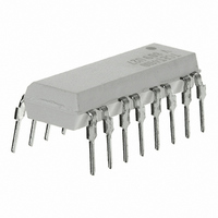
OPTOCP PHOTOTRANS 4CH 600% 16DIP
Manufacturer
Vishay
Datasheet
1.TCET4100.pdf
(9 pages)
Specifications of TCET4100
Mounting Type
Through Hole
Isolation Voltage
5000 Vrms
Number Of Channels
4
Input Type
DC
Voltage - Isolation
5000Vrms
Current Transfer Ratio (min)
50% @ 5mA
Current Transfer Ratio (max)
600% @ 5mA
Voltage - Output
70V
Current - Output / Channel
50mA
Current - Dc Forward (if)
60mA
Vce Saturation (max)
300mV
Output Type
Transistor
Package / Case
16-DIP (0.300", 7.62mm)
Maximum Input Diode Current
60 mA
Maximum Reverse Diode Voltage
6 V
Output Device
Transistor
Configuration
4
Maximum Collector Emitter Voltage
70 V
Maximum Collector Emitter Saturation Voltage
300 mV
Current Transfer Ratio
600 %
Maximum Forward Diode Voltage
1.6 V
Maximum Collector Current
50 mA
Maximum Power Dissipation
265 mW
Maximum Operating Temperature
+ 100 C
Minimum Operating Temperature
- 40 C
No. Of Channels
4
Optocoupler Output Type
Phototransistor
Input Current
50mA
Output Voltage
70V
Opto Case Style
DIP
No. Of Pins
16
Lead Free Status / RoHS Status
Lead free / RoHS Compliant
Lead Free Status / RoHS Status
Lead free / RoHS Compliant, Lead free / RoHS Compliant
Other names
751-1371-5
TCET4100
TCET4100


TCET2100 / TCET4100
Vishay Semiconductors
Switching Characteristics
www.vishay.com
4
Delay time
Rise time
Turn-on time
Storage time
Fall time
Turn-off time
Turn-on time
Turn-off time
94 9182
95 10804
300
250
200
150
100
50
0
R
0
t
T
p
t
Figure 3. Test circuit, non-saturated operation
G
p
0
Parameter
= 0.01
= 50 s
= 50 W
I
25
F
T
si
Figure 1. Derating diagram
50 W
– Safety Temperature ( °C )
I
IR-Diode
Isi ( mA )
F
50
Phototransistor
Psi ( mW )
75
100 W
100
V
(see figure 3)
V
(see figure 3)
V
(see figure 3)
V
(see figure 3)
V
(see figure 3)
V
(see figure 3)
V
(see figure 4)
V
(see figure 4)
S
S
S
S
S
S
S
S
+ 5 V
I
Channel II
= 5 V, I
= 5 V, I
= 5 V, I
= 5 V, I
= 5 V, I
= 5 V, I
= 5 V, I
= 5 V, I
C
Channel I
= 2 mA; adjusted through
125
Test condition
C
C
C
C
C
C
F
F
150
= 2 mA, R
= 2 mA, R
= 2 mA, R
= 2 mA, R
= 2 mA, R
= 2 mA, R
= 10 mA, R
= 10 mA, R
input amplitude
Oscilloscope
R
C
L
L
= 1 MW
= 20 pF
L
L
L
L
L
L
L
L
= 100 Ω
= 100 Ω
= 100 Ω
= 100 Ω
= 100 Ω
= 100 Ω
= 1 kΩ
= 1 kΩ
Figure 2. Test pulse diagram for sample test according to DIN EN
Symbol
13930
V
95 10843
t
t
t
t
V
V
t
on
t
off
on
off
t
t
IOWM
d
s
r
f
IOTM
IORM
V
Pd
0
60747-5-2(VDE0884)/ DIN EN 60747-; IEC60747
0
R
t
T
p
t
G
p
t
= 0.01
= 50 s
= 50 Ω
1
Figure 4. Test circuit, saturated operation
I
Min
F
µ
50
I
F
t
t
t
1
3
stres
Ω
t
test
= 10 mA
, t
, t
2
4
t
Tr
= 1 to 10 s
= 1 s
= 10 s
= 12 s
= 60 s
10.0
Typ.
1 k
3.0
3.0
6.0
0.3
4.7
5.0
9.0
Ω
+ 5 V
I
Channel II
Channel I
C
Document Number 83727
t
Max
2
t
3
Rev. 1.4, 26-Oct-04
t
t
stres
test
t
t
4
Oscilloscope
R
C
L
L
≥
≤
1
20 pF
M
Unit
µs
µs
µs
µs
µs
µs
µs
µs
Ω
Related parts for TCET4100
Image
Part Number
Description
Manufacturer
Datasheet
Request
R

Part Number:
Description:
357-036-542-201 CARDEDGE 36POS DL .156 BLK LOPRO
Manufacturer:
Vishay
Datasheet:
Part Number:
Description:
357-036-542-201 CARDEDGE 36POS DL .156 BLK LOPRO
Manufacturer:
Vishay
Datasheet:
Part Number:
Description:
357-036-542-201 CARDEDGE 36POS DL .156 BLK LOPRO
Manufacturer:
Vishay
Datasheet:
Part Number:
Description:
357-036-542-201 CARDEDGE 36POS DL .156 BLK LOPRO
Manufacturer:
Vishay
Datasheet:
Part Number:
Description:
357-036-542-201 CARDEDGE 36POS DL .156 BLK LOPRO
Manufacturer:
Vishay
Datasheet:
Part Number:
Description:
357-036-542-201 CARDEDGE 36POS DL .156 BLK LOPRO
Manufacturer:
Vishay
Datasheet:
Part Number:
Description:
357-036-542-201 CARDEDGE 36POS DL .156 BLK LOPRO
Manufacturer:
Vishay
Datasheet:
Part Number:
Description:
357-036-542-201 CARDEDGE 36POS DL .156 BLK LOPRO
Manufacturer:
Vishay
Datasheet:
Part Number:
Description:
357-036-542-201 CARDEDGE 36POS DL .156 BLK LOPRO
Manufacturer:
Vishay
Datasheet:
Part Number:
Description:
357-036-542-201 CARDEDGE 36POS DL .156 BLK LOPRO
Manufacturer:
Vishay
Datasheet:
Part Number:
Description:
357-036-542-201 CARDEDGE 36POS DL .156 BLK LOPRO
Manufacturer:
Vishay
Datasheet:
Part Number:
Description:
357-036-542-201 CARDEDGE 36POS DL .156 BLK LOPRO
Manufacturer:
Vishay
Datasheet:
Part Number:
Description:
357-036-542-201 CARDEDGE 36POS DL .156 BLK LOPRO
Manufacturer:
Vishay
Datasheet:
Part Number:
Description:
357-036-542-201 CARDEDGE 36POS DL .156 BLK LOPRO
Manufacturer:
Vishay
Datasheet:
Part Number:
Description:
357-036-542-201 CARDEDGE 36POS DL .156 BLK LOPRO
Manufacturer:
Vishay
Datasheet: