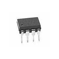
HCPL-7560-560E Avago Technologies US Inc., HCPL-7560-560E Datasheet - Page 7

HCPL-7560-560E
Manufacturer Part Number
HCPL-7560-560E
Description
OPTOCOUPLER MODULE IEC 8-SMD
Manufacturer
Avago Technologies US Inc.
Type
Sigma-Delta Modulatorr
Datasheet
1.HCPL-7560-500E.pdf
(18 pages)
Specifications of HCPL-7560-560E
Voltage - Isolation
3750Vrms
Input Type
DC
Voltage - Supply
4.5 V ~ 5.5 V
Operating Temperature
-40°C ~ 85°C
Mounting Type
Surface Mount
Package / Case
8-SMD Gull Wing
No. Of Channels
1
Input Current
20mA
Output Voltage
6V
Opto Case Style
SMD
No. Of Pins
8
Peak Reflow Compatible (260 C)
Yes
Input Current Max
20mA
Reel Quantity
1000
Isolation Voltage
3.75kV
Lead Free Status / RoHS Status
Lead free / RoHS Compliant
Available stocks
Company
Part Number
Manufacturer
Quantity
Price
Company:
Part Number:
HCPL-7560-560E
Manufacturer:
AVAGO
Quantity:
40 000
Electrical Specifications (DC)
Unless otherwise noted, all specifications are at V
and V
+85°C, V
Electrical Specifications (Tested with HCPL-0872 or Sinc
Unless otherwise noted, all specifications are at V
specifications are at T
over the following ranges: T
7
Parameter
Average Input Bias Current
Average Input Resistance
Input DC Common-Mode Rejection
Ratio
Output Logic High Voltage
Output Logic Low Voltage
Output Short Circuit Current
Input Supply Current
Output Supply Current
Output Clock Frequency
Data Hold Time
Parameter
STATIC CHARACTERISTICS
Resolution
Integral Nonlinearity
Differential Nonlinearity
Uncalibrated Input Offset
Offset Drift vs. Temperature
Offset drift vs. VDD1
Internal Reference Voltage
Absolute Reference Voltage
Tolerance
VREF Drift vs. Temperature
VREF Drift vs. VDD1
Full Scale Input Range
Recommended Input Voltage
Range
DD1
DD1
= V
= 4.5 to 5.5 V and V
DD2
= 5 V, and all Minimum and Maximum specifications apply over the following ranges: T
A
= 25°C and V
A
DD2
= -40°C to +85°C, V
Symbol
INL
DNL
V
dV
dV
V
dV
dV
OS
REF
= 4.5 to 5.5 V.
OS
OS
REF
REF
/dT
/dV
/dT
/dV
DD1
Symbol
I
R
CMRR
V
V
|I
I
I
f
t
IN
DD1
DD2
CLK
HDDAT
OSC
IN
OH
OL
A
DD1
A
DD1
= V
|
IN
DD2
Min.
15
-6
-5
-V
-200
3
IN+
Min.
3.9
7.5
REF
Filter)
= 5 V, and all Minimum and Maximum specifications apply
DD1
= 0 V and V
IN+
Typ.
64
0.2
0
2
0.12
320
150
0.2
= 4.5 to 5.5 V and V
= -200 mV to +200 mV and V
Typ.
-0.8
450
60
4.9
0.1
30
10
10
10
15
Max.
256
0.8
1
6
35
5
+V
+200
IN-
Max.
0.6
20
20
15
REF
= 0 V, all Typical specifications are at T
Units
bits
LSB
%
LSB
mV
µV/°C
mV/V
mV
%
ppm/°C.
%
mV
mV
Units
µA
k W
dB
V
V
mA
mA
mA
MHz
ns
DD2
= 4.5 to 5.5 V.
Conditions
I
I
V
or GND2
V
to +350 mV
OUT
OUT
OUT
IN+
Conditions
V
V
V
IN+
IN+
IN+
= -100 µA
= 1.6 mA
= -350 mV
IN-
= V
= 0 V
= 0 V
= 0 V
= 0 V; all Typical
DD2
Fig.
5
6
7
7
7
8
8
8
8
Fig.
1
2
3
4
A
= -40°C to
A
Note
7
8
8
9
10
11
Note
3
3
4
5
6
= 25°C


