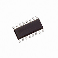
HCPL-788J#500 Avago Technologies US Inc., HCPL-788J#500 Datasheet - Page 15

HCPL-788J#500
Manufacturer Part Number
HCPL-788J#500
Description
OPTOCOUPLR AMP CURR SENSE 16SMD
Manufacturer
Avago Technologies US Inc.
Type
Current Sensorr
Datasheet
1.HCPL-788J-000E.pdf
(20 pages)
Specifications of HCPL-788J#500
Voltage - Isolation
3750Vrms
Input Type
DC
Voltage - Supply
4.5 V ~ 5.5 V
Operating Temperature
-40°C ~ 85°C
Mounting Type
Surface Mount
Package / Case
16-SOIC (0.300", 7.5mm Width)
Package Type
SOIC
Operating Supply Voltage (typ)
5V
Lead Free Status / RoHS Status
Contains lead / RoHS non-compliant
Available stocks
Company
Part Number
Manufacturer
Quantity
Price
An inexpensive 78L05 three-terminal regulator can also
be used to reduce the floating supply voltage to 5 V. To
help attenuate high-frequency power supply noise or
ripple, a resistor or inductor can be used in series with
the input of the regulator to form a low-pass filter with
the regulator’s input bypass capacitor.
As shown in Figure 25, 0.1 μF bypass capacitors (C1, C3,
C4, and C6) should be located as close as possible to the
pins of the HCPL-788J. The bypass capacitors are required
because of the high-speed digital nature of the signals
inside the HCPL-788J. A 0.01 μF bypass capacitor (C2) is
also recommended at the input due to the switched-ca-
pacitor nature of the input circuit. The input bypass ca-
pacitor also forms part of the anti-aliasing filter, which
is recommended to prevent high-frequency noise from
aliasing down to lower frequencies and interfering with
the input signal. The input filter also performs an impor-
tant reliability function — it reduces transient spikes
from ESD events flowing through the current sensing
resistor.
Figure 27. Example printed circuit board layout.
15
BOTTOM LAYER
TOP LAYER
PC Board Layout
The design of the printed circuit board (PCB) should fol-
low good layout practices, such as keeping bypass ca-
pacitors close to the supply pins, keeping output signals
away from input signals, the use of ground and power
planes, etc. In addition, the layout of the PCB can also af-
fect the isolation transient immunity (CMTI) of the HCPL-
788J, due primarily to stray capacitive coupling between
the input and the output circuits. To obtain optimal CMTI
performance, the layout of the PC board should mini-
mize any stray coupling by maintaining the maximum
possible distance between the input and output sides of
the circuit and ensuring that any ground or power plane
on the PC board does not pass directly below or extend
much wider than the body of the HCPL-788J.


