TLP2630 Toshiba, TLP2630 Datasheet - Page 4
TLP2630
Manufacturer Part Number
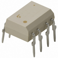
TLP2630
Description
PHOTOCOUPLER DUAL 6N137 8-DIP
Manufacturer
Toshiba
Specifications of TLP2630
Voltage - Isolation
2500Vrms
Number Of Channels
2, Unidirectional
Current - Output / Channel
16mA
Data Rate
10MBd
Propagation Delay High - Low @ If
60ns @ 0 ~ 7.5mA
Current - Dc Forward (if)
20mA
Input Type
DC
Output Type
Open Collector
Mounting Type
Through Hole
Package / Case
8-DIP (0.300", 7.62mm)
No. Of Channels
2
Isolation Voltage
2.5kV
Optocoupler Output Type
Logic Gate
Input Current
15mA
Output Voltage
5.5V
Opto Case Style
DIP
No. Of Pins
8
Approval Category
UL1577
Rohs Compliant
Yes
Lead Free Status / RoHS Status
Contains lead / RoHS non-compliant
Available stocks
Company
Part Number
Manufacturer
Quantity
Price
Company:

Part Number:
TLP2630
Manufacturer:
TOS
Quantity:
2 988
Part Number:
TLP2630
Manufacturer:
TOSHIBA/东芝
Quantity:
20 000


Switching Characteristics
Propagation delay time to
low output level
Propagation delay time to
high output level
Output rise a time,output
fall time(10~90%)
Common mode transient
immunity at high output
level
Common mode transient
immunity at low output
level
(Note 1) 2mm below seating plane.
(Note 2) The V
(Note 3) Device considered a two-terminal device: Pins 1, 2, 3 and 4 shorted together, and pins 5, 6, 7 and 8
(Note 4) CM
(Note 5) CM
(Note 6) Measured between pins 1 and 2 shorted together, and pins 3 and 4 shorted together.
Characteristic
larger.This can be either a ceramic or solid tantalum capacitor with good high frequency characteristic
and should be connected as close as possible to the package V
shorted together.
remain in the high state(i.e., V
in the low output state(i.e., V
Measured in volts per microsecond(V / µs).
H
L
・the maximum tolerable rate of fall of the common mode voltage to ensure the output will remain
・the maximum tolerable rate of rise of the common mode voltage to ensure the output will
CC
supply voltage to each TLP2630 isolator must be bypassed by a 0.01µF capacitor or
Symbol
CM
CM
t
t
pHL
pLH
t
r
,t
f
H
L
(Ta =25°C , V
Test
Cir-
cuit
1
1
1
2
2
OUT
OUT
> 0.8V)
I
C
I
C
I
C
I
V
V
I
V
V
> 2.0V)
F
F
F
F
F
L
L
L
CM
O
CM
O
CC
= 0®7.5mA, R
= 7.5mA®0, R
= 0
= 0, R
= 7.5mA, R
(min.) = 2V
(max.) = 0.8V
= 15pF (each channel)
= 15pF (each channel)
= 15pF (each channel)
= 200V
= 200V
=5V)
(each channel, Note 4)
(each channel, Note 5)
Test Condition
4
L
7.5mA, R
= 350Ω
L
= 350Ω
L
L
L
= 350Ω
= 350Ω
= 350Ω
Min.
CC
¾
¾
¾
¾
¾
and GND pins each device.
-500
Typ.
200
60
60
30
Max.
75
75
¾
¾
¾
V / µs
V / µs
Unit
ns
ns
ns
2002-09-25
TLP2630
Related parts for TLP2630
Image
Part Number
Description
Manufacturer
Datasheet
Request
R

Part Number:
Description:
Toshiba Semiconductor [TOSHIBA IGBT Module Silicon N Channel IGBT]
Manufacturer:
TOSHIBA Semiconductor CORPORATION
Datasheet:
Part Number:
Description:
TOSHIBA GTR MODULE SILICON NPN TRIPLE DIFFUSED TYPE
Manufacturer:
TOSHIBA Semiconductor CORPORATION
Datasheet:
Part Number:
Description:
TOSHIBA GTR Module Silicon N Channel IGBT
Manufacturer:
TOSHIBA Semiconductor CORPORATION
Datasheet:
Part Number:
Description:
TOSHIBA Intelligent Power Module Silicon N Channel IGBT
Manufacturer:
TOSHIBA Semiconductor CORPORATION
Datasheet:
Part Number:
Description:
TOSHIBA INTELLIGENT POWER MODULE SILICON N CHANNEL LGBT
Manufacturer:
TOSHIBA Semiconductor CORPORATION
Datasheet:
Part Number:
Description:
TOSHIBA IGBT Module Silicon N Channel IGBT
Manufacturer:
TOSHIBA Semiconductor CORPORATION
Datasheet:
Part Number:
Description:
TOSHIBA GTR MODULE SILICON N−CHANNEL IGBT
Manufacturer:
TOSHIBA Semiconductor CORPORATION
Datasheet:
Part Number:
Description:
TOSHIBA Intelligent Power Module Silicon N Channel IGBT
Manufacturer:
TOSHIBA Semiconductor CORPORATION
Datasheet:
Part Number:
Description:
TOSHIBA GTR Module Silicon N Channel IGBT
Manufacturer:
TOSHIBA Semiconductor CORPORATION
Datasheet:
Part Number:
Description:
TOSHIBA INTELLIGENT POWER MODULE
Manufacturer:
TOSHIBA Semiconductor CORPORATION
Datasheet:
Part Number:
Description:
TOSHIBA Intelligent Power Module Silicon N Channel IGBT
Manufacturer:
TOSHIBA Semiconductor CORPORATION
Datasheet:
Part Number:
Description:
TOSHIBA Intelligent Power Module Silicon N Channel IGBT
Manufacturer:
TOSHIBA Semiconductor CORPORATION
Datasheet:
Part Number:
Description:
TOSHIBA IGBT Module Silicon N Channel IGBT
Manufacturer:
TOSHIBA Semiconductor CORPORATION
Datasheet:
Part Number:
Description:
TOSHIBA Intelligent Power Module Silicon N Channel IGBT
Manufacturer:
TOSHIBA Semiconductor CORPORATION
Datasheet:
Part Number:
Description:
Toshiba Semiconductor [SILICON N CHANNEL 1GBT]
Manufacturer:
TOSHIBA Semiconductor CORPORATION
Datasheet: