TLP2630 Toshiba, TLP2630 Datasheet - Page 2
TLP2630
Manufacturer Part Number
TLP2630
Description
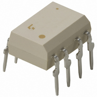
PHOTOCOUPLER DUAL 6N137 8-DIP
Manufacturer
Toshiba
Specifications of TLP2630
Voltage - Isolation
2500Vrms
Number Of Channels
2, Unidirectional
Current - Output / Channel
16mA
Data Rate
10MBd
Propagation Delay High - Low @ If
60ns @ 0 ~ 7.5mA
Current - Dc Forward (if)
20mA
Input Type
DC
Output Type
Open Collector
Mounting Type
Through Hole
Package / Case
8-DIP (0.300", 7.62mm)
No. Of Channels
2
Isolation Voltage
2.5kV
Optocoupler Output Type
Logic Gate
Input Current
15mA
Output Voltage
5.5V
Opto Case Style
DIP
No. Of Pins
8
Approval Category
UL1577
Rohs Compliant
Yes
Lead Free Status / RoHS Status
Contains lead / RoHS non-compliant
Available stocks
Company
Part Number
Manufacturer
Quantity
Price
Company:

Part Number:
TLP2630
Manufacturer:
TOS
Quantity:
2 988
Part Number:
TLP2630
Manufacturer:
TOSHIBA/东芝
Quantity:
20 000


Absolute Maximum Ratings
Recommended Operating Conditions
Operating temperature range
Storage temperature range
Lead soldering temperature (10 s)
Isolation voltage
Note: Using continuously under heavy loads (e.g. the application of high temperature/current/voltage and the
Input current, low level, each channel
Input current, high level, each channel
Supply voltage**, output
Fan out(TTL load, each channel)
Operating temperature
Note: Recommended operating conditions are given as a design guideline to obtain expected performance of the
* t ≤ 1 msec duration.
* 6.3mA is a guard banded value which allows for at least 20% CTR degradation.
**This item denotes operating ranges, not meaning of recommended operating conditions.
Initial input current threshold value is 5.0mA or less.
Forward current(each channel)
Pulse forward current
(each channel)*
Reverse voltage(each channel)
Output current(each channel)
Output voltage(each channel)
Supply voltage
(1 minute maximum)
Output collector power
dissipation(each channel)
significant change in temperature, etc.) may cause this product to decrease in the reliability significantly even
if the operating conditions (i.e. operating temperature/current/voltage, etc.) are within the absolute maximum
ratings and the operating ranges.
Please design the appropriate reliability upon reviewing the Toshiba Semiconductor Reliability Handbook
(“Handling Precautions”/“Derating Concept and Methods”) and individual reliability data (i.e. reliability test
report and estimated failure rate, etc).
device. Additionally, each item is an independent guideline respectively. In developing designs using this
product, please confirm specified characteristics shown in this document.
Characteristic
Characteristic
(AC, 1 min., R.H.≤ 60%, Note 3)
(no derating required up to 70°C)
Symbol
V
T
I
I
FH
FL
N
CC
opr
(Note 1)
6.3*
Min
4.5
⎯
0
0
Symbol
V
BV
T
T
T
I
V
P
V
2
I
I
FP
opr
CC
stg
sol
O
F
R
O
O
S
Typ.
⎯
⎯
⎯
⎯
5
−55 to 125
−40 to 85
−0.5 to 7
Rating
2500
260
20
30
16
40
Max
250
5
7
5.5
15
70
8
Unit
mA
μA
°C
V
Vrms
Unit
mW
mA
mA
mA
°C
°C
°C
V
V
V
2007-10-01
TLP2630
Related parts for TLP2630
Image
Part Number
Description
Manufacturer
Datasheet
Request
R

Part Number:
Description:
Toshiba Semiconductor [TOSHIBA IGBT Module Silicon N Channel IGBT]
Manufacturer:
TOSHIBA Semiconductor CORPORATION
Datasheet:
Part Number:
Description:
TOSHIBA GTR MODULE SILICON NPN TRIPLE DIFFUSED TYPE
Manufacturer:
TOSHIBA Semiconductor CORPORATION
Datasheet:
Part Number:
Description:
TOSHIBA GTR Module Silicon N Channel IGBT
Manufacturer:
TOSHIBA Semiconductor CORPORATION
Datasheet:
Part Number:
Description:
TOSHIBA Intelligent Power Module Silicon N Channel IGBT
Manufacturer:
TOSHIBA Semiconductor CORPORATION
Datasheet:
Part Number:
Description:
TOSHIBA INTELLIGENT POWER MODULE SILICON N CHANNEL LGBT
Manufacturer:
TOSHIBA Semiconductor CORPORATION
Datasheet:
Part Number:
Description:
TOSHIBA IGBT Module Silicon N Channel IGBT
Manufacturer:
TOSHIBA Semiconductor CORPORATION
Datasheet:
Part Number:
Description:
TOSHIBA GTR MODULE SILICON N−CHANNEL IGBT
Manufacturer:
TOSHIBA Semiconductor CORPORATION
Datasheet:
Part Number:
Description:
TOSHIBA Intelligent Power Module Silicon N Channel IGBT
Manufacturer:
TOSHIBA Semiconductor CORPORATION
Datasheet:
Part Number:
Description:
TOSHIBA GTR Module Silicon N Channel IGBT
Manufacturer:
TOSHIBA Semiconductor CORPORATION
Datasheet:
Part Number:
Description:
TOSHIBA INTELLIGENT POWER MODULE
Manufacturer:
TOSHIBA Semiconductor CORPORATION
Datasheet:
Part Number:
Description:
TOSHIBA Intelligent Power Module Silicon N Channel IGBT
Manufacturer:
TOSHIBA Semiconductor CORPORATION
Datasheet:
Part Number:
Description:
TOSHIBA Intelligent Power Module Silicon N Channel IGBT
Manufacturer:
TOSHIBA Semiconductor CORPORATION
Datasheet:
Part Number:
Description:
TOSHIBA IGBT Module Silicon N Channel IGBT
Manufacturer:
TOSHIBA Semiconductor CORPORATION
Datasheet:
Part Number:
Description:
TOSHIBA Intelligent Power Module Silicon N Channel IGBT
Manufacturer:
TOSHIBA Semiconductor CORPORATION
Datasheet:
Part Number:
Description:
Toshiba Semiconductor [SILICON N CHANNEL 1GBT]
Manufacturer:
TOSHIBA Semiconductor CORPORATION
Datasheet: